
Wiring board construction and methods of making same

a wiring board and wire technology, applied in the field of wiring board construction, can solve the problems of time-consuming and expensive, forming through holes by drilling through the pads individually, and reducing so as to increase the wiring capacity of the board, little or no loss in valuable spa

Inactive Publication Date: 2004-09-14
DIMENSIONAL CIRCUITS
View PDF8 Cites 1 Cited by
  • Summary
  • Abstract
  • Description
  • Claims
  • Application Information

AI Technical Summary

Benefits of technology

Therefore, the principal object of the present invention is to provide a new and improved wiring board construction and method of making it, wherein microvias can be formed simultaneously without individual drilling and with little or no loss in valuable space on the wiring board, thereby to increase the wiring capacity for the board.
Briefly, the above and further objects of the present invention are realized by providing a new and improved wiring board and construction and method of making it to produce wiring board constructions having high density microvias formed without occupying unnecessary space on the board. Surrounding pads are either greatly reduced in size or entirely eliminated. Furthermore, the microvias are all able to be formed simultaneously, without the requirement of expensive individual drilling, and are formed at the same time as the traces on the board.
A wiring board construction includes at least one microvia disposed in a base substrate and includes a deep imprinted recess in the top surface thereof. A conductor material is disposed within the recess, and has a portion disposed at the bottom thereof. A conductor disposed at a bottom surface of the substrate opposite to the conductor material bottom portion helps to complete an electrically conductor path through the substrate to help complete an electrically conductive path through the substrate.

Problems solved by technology

As explained in the book, entitled "Printed Circuit Handbook", Fourth Edition, by Clyde F. Coombs, Jr., published by McGraw-Hill, the misregistration is caused principally by the instability and movement of the base laminate substrate during the process of making the printed wiring board or multilayer board.
By having the large pad surrounding the hole, an unwanted and undesirable waste of valuable space on the wiring board results.
Additionally, the forming of through holes by drilling through the pads individually is time consuming and expensive.

Method used


Image

  • Wiring board construction and methods of making same
  • Wiring board construction and methods of making same
  • Wiring board construction and methods of making same

Examples


Embodiment Construction

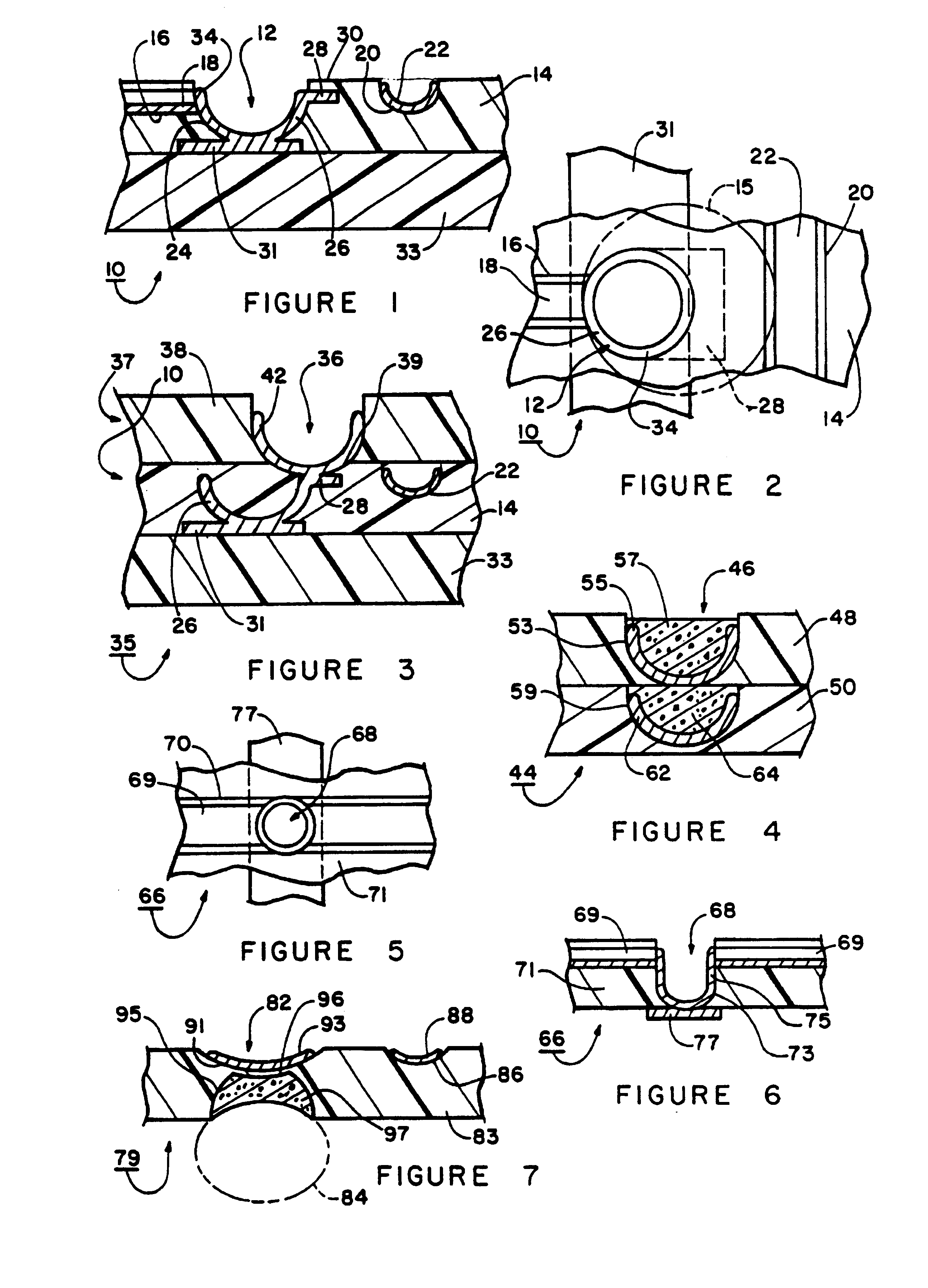
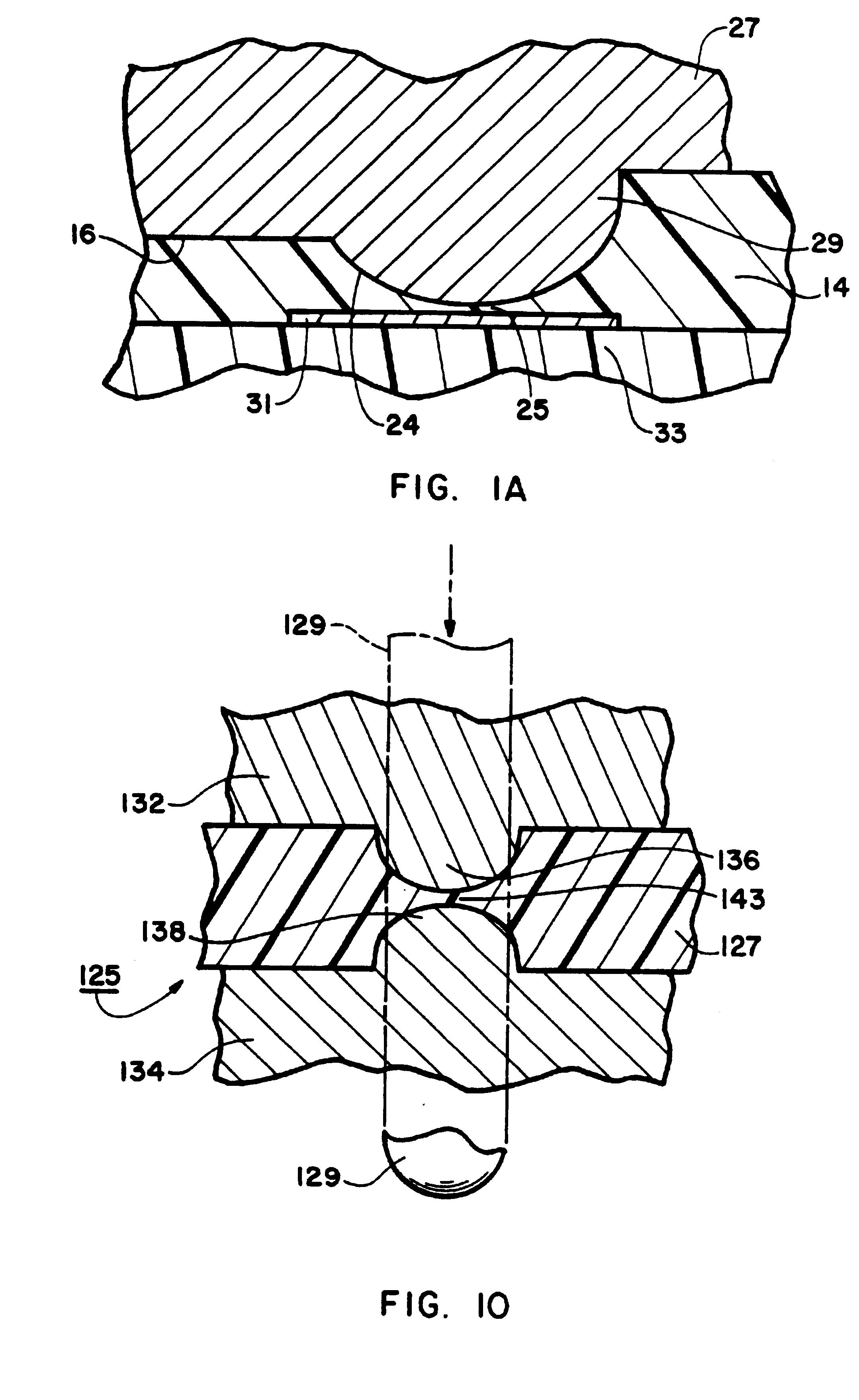
Referring now to the drawings, and more particularly to FIGS. 1, 1A and 2 thereof, there is shown a wiring board construction 10, which is constructed in accordance with the present invention. The terms "wiring board" as used herein are intended to refer to and to include the terms "printed circuit board."

The wiring board construction 10 includes a microvia 12 formed in the wiring board construction 10 in accordance with the present invention. As seen in FIG. 2, the size of the microvia 12 is substantially smaller than the size of a conventional pad as indicated at 15 which would surround a conventional microvia (not shown), thereby greatly improving wiring density for the wiring board construction 10 as compared with conventional wiring densities.

A conductor shallow groove 16 has a conductor pad 18 or trace electrically connected to the microvia 12. The curved conductor trace 18 is formed in the top substrate 14 in accordance with fabrication methods disclosed in U.S. Pat. Nos. 5,3...


PUM

PropertyMeasurementUnit
diameteraaaaaaaaaa
electrically conductiveaaaaaaaaaa
compressibleaaaaaaaaaa

Abstract

A wiring board construction includes at least one microvia disposed in a base substrate and includes a deep imprinted cup shaped recess in the top surface thereof. A conductor material is disposed within the recess, and has a portion disposed at the bottom thereof. A conductor disposed at a bottom surface of the substrate opposite to the conductor material bottom portion helps to complete an electrically conductor path through the substrate to help complete an electrically conductive path through the substrate.

Description

REFERENCE TO A "MICROFICHE APPENDIX"Not applicableBACKGROUND OF THE INVENTION1. Technical FieldThe present invention relates in general to wiring board constructions and methods of making them. The invention more particularly relates to methods of making microvias in wiring boards.2. Background ArtPlated through holes have been employed in printed wiring boards for establishing electrical connections between the top and bottom sides of the boards. Such plated through holes have also been employed in multiple layer wiring board constructions.According to the construction of conventional plated through holes, relatively large pads surround the plated through holes according to conventional design techniques, because the plated through holes are created by drilling through the conductor pad and the board. The pad is electrically connected to a conductor trace, and the conventional pads are substantially larger in size than the trace to accommodate any potential layer-to-layer or patter...

Claims


Application Information

Patent Timeline
Patent Type & Authority Patents(United States)
IPC IPC(8): H01R12/55H05K1/09H05K1/11H05K3/00H05K3/06H05K3/10H05K3/12H05K3/40H05K3/46
CPCH05K1/115H05K3/005H05K3/107H05K3/4652H05K1/095Y10T29/49167H05K3/0014H05K3/061H05K3/1241H05K3/4069H05K3/4614H05K3/4617H05K3/465H05K2201/0394H05K2201/09036H05K2201/09472H05K2201/09509H05K2201/0959H05K2201/096H05K2201/09863H05K2201/09981H05K2203/0108H05K2203/025H05K2203/041H05K2203/0746H05K2203/095H05K2203/1189H05K2203/1572Y10T29/49126Y10T29/49158Y10T29/49165H05K1/112
Inventor GREGOIRE, GEORGE D.
Owner DIMENSIONAL CIRCUITS
Learn More