Magnet logic element and magnet logic element array

A technology of logic components and magnetic bodies, which can be applied to magnetic objects, logic circuits using magnetic saturation devices, logic circuits, etc., and can solve problems such as reducing the size of multiple components

Inactive Publication Date: 2007-11-28
KK TOSHIBA
View PDF5 Cites 0 Cited by
  • Summary
  • Abstract
  • Description
  • Claims
  • Application Information

AI Technical Summary

Problems solved by technology

On the other hand, although conventional logic circuits are formed of semiconductors, there are problems such as size reduction and multi-element configuration for further miniaturization and integration in the future.

Method used


Image

  • Magnet logic element and magnet logic element array
  • Magnet logic element and magnet logic element array
  • Magnet logic element and magnet logic element array

Examples


Embodiment

[0225] Hereinafter, embodiments of the present invention will be described in more detail with reference to examples.

no. 1 example

[0227] First, as a first example of the present invention, an element CL having a double tunnel junction having the cross-sectional structure illustrated in FIG. 25 was fabricated. As shown in FIG. 26, this element CL performs signal input using a current magnetic field using a bit line BL and a word line WL.

[0228] In addition, in the element array shown in FIG. 26, in addition to the constituent elements shown in the figure, transistors for cell selection are arranged in each cell, and word lines for selecting these transistors are provided.

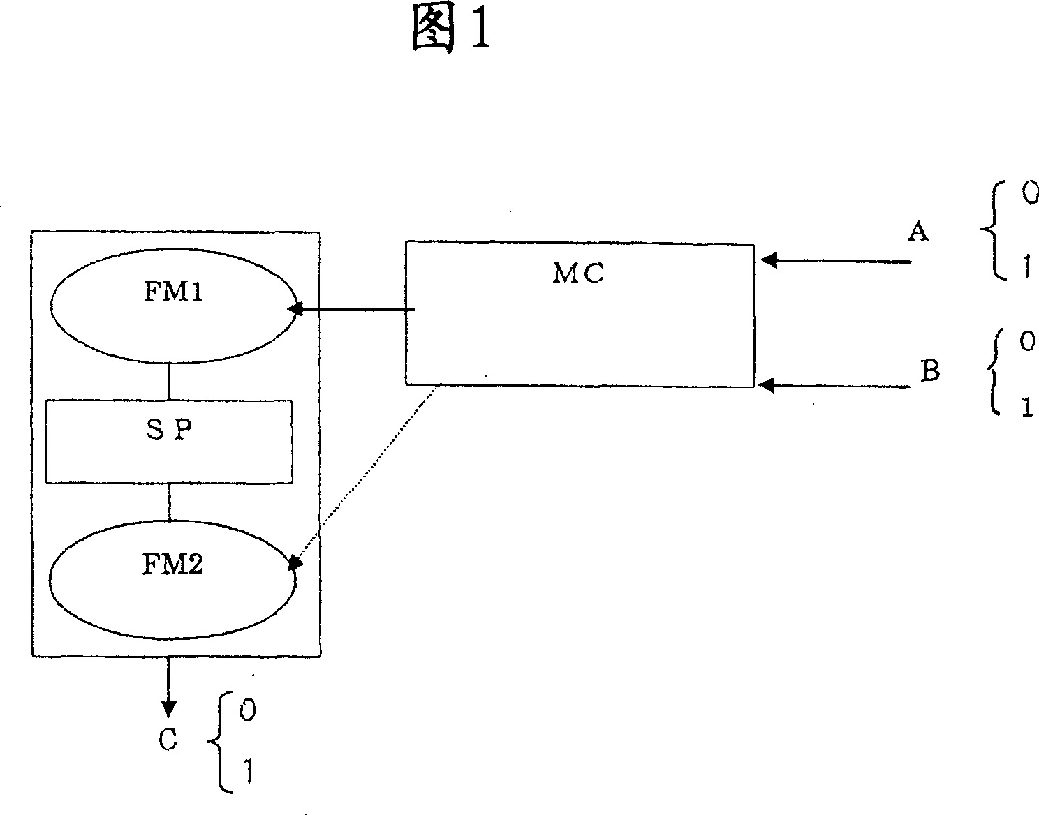
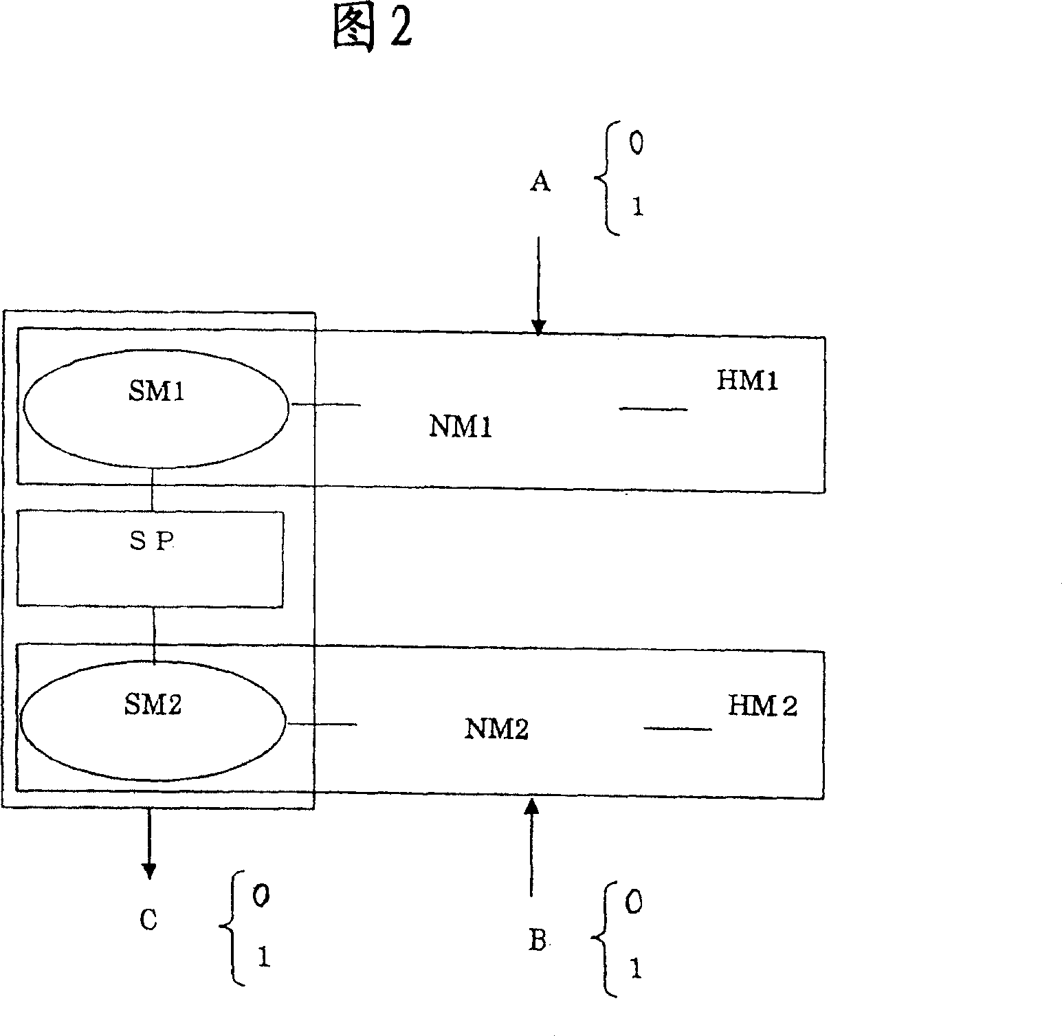
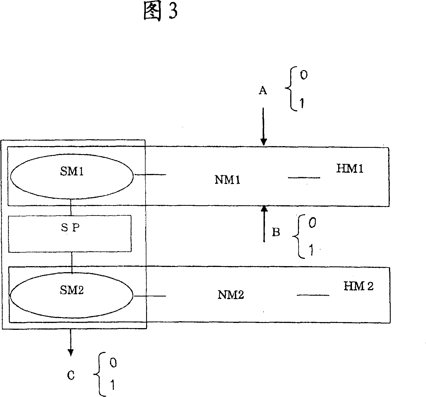
[0229] Here, the magnetic body in the center of the element CL having a double tunnel junction is a soft magnetic unit SM, and the magnetization of this layer SM is changed according to the change of the combined magnetic field formed by the bit line BL and the word line WL according to the input signal.

[0230] In addition, the magnetization directions of the semi-hard layers HM1 and HM2 on the upper and lower sides of the element ...

no. 2 example

[0234] Next, as a second embodiment of the present invention, two elements of the above-mentioned first embodiment were combined to manufacture an EOR memory for recording that performs one EOR process. Here, the magnetization of the semi-hard layers HM1, HM2 is programmed to be directed to the right in FIG. 22 . Then, first initialize the magnetization of the soft magnetic unit SM so that its direction is to the right, then input the signal A and signal B directly into the first unit, and input both the signals A and B into the second unit after inversion . According to the magnetization configuration obtained as a result thereof, the truth table is shown in FIG. 24 . If a data signal is input as signal A and a cipher signal is input as signal B, then with these two unit 1-bit elements, data can be stored as a stream cipher. If the signal B is "0", reproduction is performed by reading two cells, and if the signal B is "1", reproduction is performed by reading one cell.


PUM


Abstract

The technical subject of the present invention is to provide a novel magnetic logic element which is small and can perform logic processing, and magnetic logic element array formed by arrange the device in an array. The means to solve the said technical subject of the present invention is to provide a magnetic logic element comprising: at least two magnetic layers (HM, SM); an intermediate portion (SP) between the magnetic layer; and the magnetization direction controlling portion of the magnetic layer (SM); and more than two input signals A, B for controlling the magnetization direction of the magnetic layer (SM), which are assigned with logic 0, 1 to determine the magnetization of the magnetic layer (SM) by the configuration of the input signals A, B. The magnitude of the magnetoresistance effect of the intermediate portion inbetween is the output signal C.

Description

[0001] (Cross-reference to related application [0002] This application is based on and claims priority from prior Japanese Application No. 2002-097445 filed on March 29, 2001, the entire contents of which are incorporated herein by reference. ) technical field [0003] The present invention relates to a magnetic logic element and a magnetic logic element array, and more specifically, to a current direct drive type recording and a magnetic logic element and a magnetic logic element array capable of reproducing by utilizing the magnetoresistance effect. Background technique [0004] In a lamination structure composed of ferromagnetic layer / nonmagnetic layer / ferromagnetic layer, when a current flows in-plane, a giant magnetoresistance effect is found, and since this discovery, as a material with a large magnetoresistance In the system of change rate, the CPP (Current Perpendicular to Plane) type magnetoresistance effect element in which the current flows in the direction per...

Claims


Application Information

Patent Timeline
Patent Type & Authority Patents(China)
IPC IPC(8): G11C11/15H01L43/00H03K19/16G11C11/16H03K19/168
CPCG11C11/16B82Y25/00H01F10/3263H03K19/168G11C11/161G11C11/1673G11C11/1675G11C11/15
Inventor 中村志保羽根田茂
Owner KK TOSHIBA
Why Eureka
Try Eureka