Method and apparatus for producing polysilicon film, semiconductor device, and manufacture thereof
A manufacturing method and a manufacturing device technology, which are applied in the field of polycrystalline silicon film manufacturing and manufacturing devices, and can solve the problems of small second harmonic output, difficult polycrystalline silicon film manufacturing, etc.
- Summary
- Abstract
- Description
- Claims
- Application Information
AI Technical Summary
Problems solved by technology
Method used
Image

Examples
Embodiment approach 1
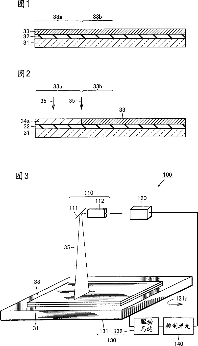
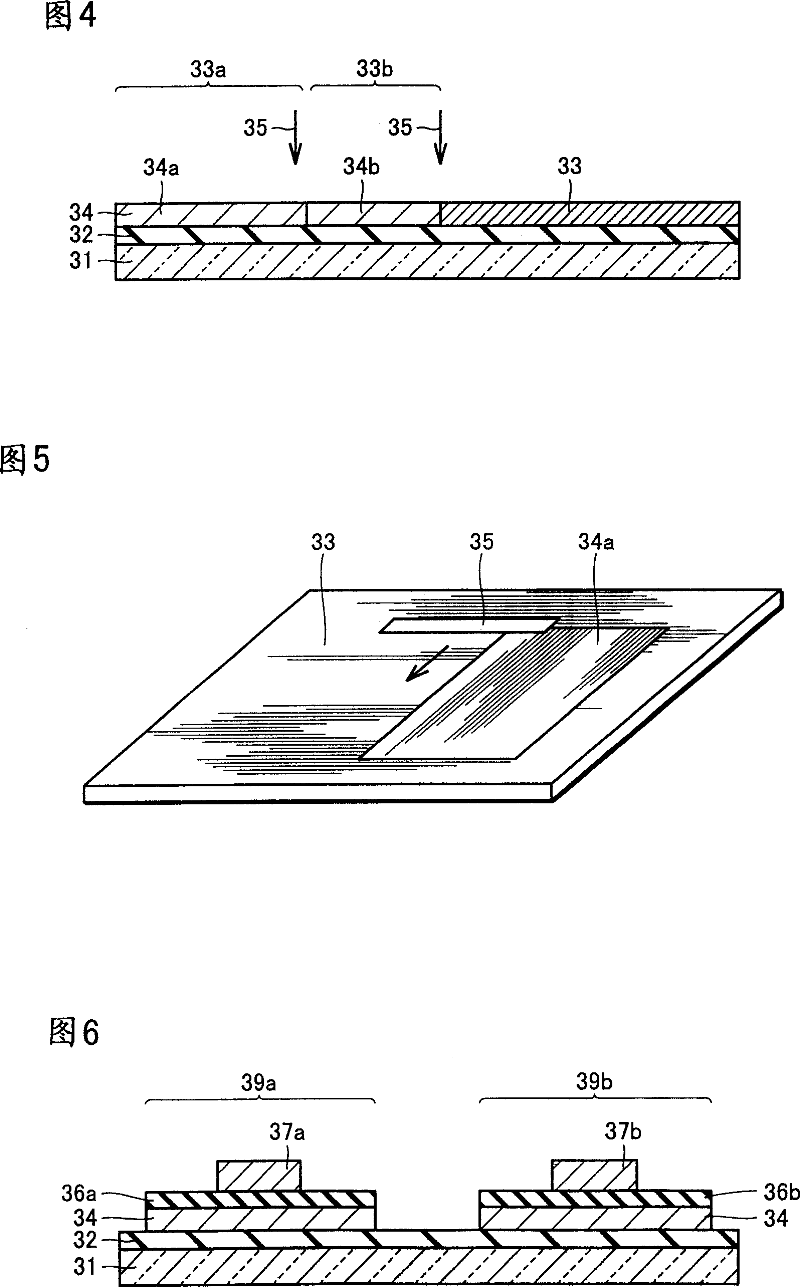
[0061] 1 to 6 are diagrams showing a method of manufacturing a polycrystalline silicon film according to Embodiment 1 of the present invention. As shown in FIG. 1, a silicon oxide film 32 is formed on a glass substrate 31 by, for example, CVD. An amorphous silicon film 33 is formed on the silicon oxide film 32 by CVD. The amorphous silicon film 33 has a first region 33a and a second region 33b in contact with the first region 33a.
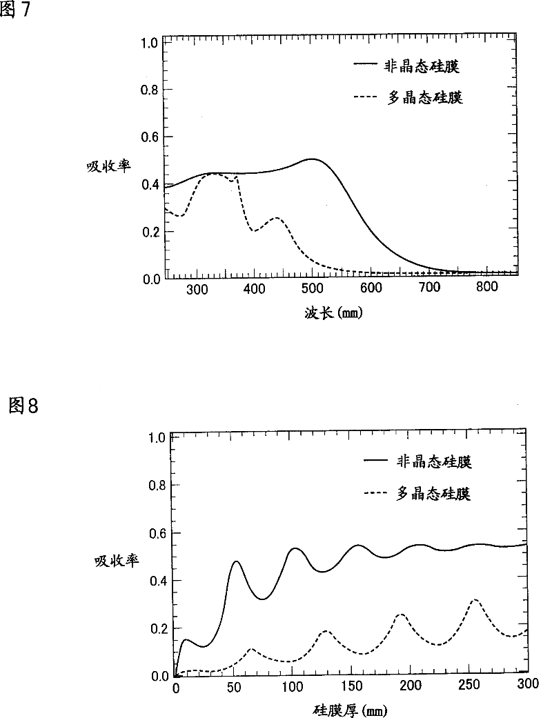
[0062] As shown in FIGS. 2 and 3 , second harmonic laser light (wavelength 523 nm) of Q-switched Nd:YAG is irradiated on the first region 33 a of the amorphous silicon film 33 . As a result, the portion irradiated with the laser light 35 is polycrystallized to form the first polycrystalline portion 34a. At this time, the apparatus shown in FIG. 3 was used for laser irradiation.
[0063]As shown in Figure 3, the manufacturing apparatus 100 of polycrystalline silicon film comprises: the oscillator 120 that oscillates and produces the laser light o...
Embodiment approach 2
[0090] 13 is a perspective view showing a method of manufacturing a polycrystalline silicon film according to Embodiment 2 of the present invention. In the polycrystalline silicon film manufacturing apparatus 180 shown in FIG. 13 , the polycrystalline silicon film shown in FIG. The irradiation unit is different from the film production apparatus 100 . That is, in the polycrystalline silicon film manufacturing apparatus 180 shown in FIG. 13, as the irradiation unit, there are a first irradiation unit 110a, a second irradiation unit 110b, and a third irradiation unit 110c. The first, second, and third irradiation units 110a, 110b, and 110c are composed of a mirror 111 and a beam shaping optical system 112, respectively. The mirror 111 and the beam shaping optical system 112 are the same as those shown in FIG. 3 . Each beam shaping optical system 112 is connected to a laser oscillator 120a as a first oscillating unit, a laser oscillator 120b as a second oscillating unit, and a l...
Embodiment approach 3
[0098] Fig. 17 is an oblique view showing a polycrystalline silicon film manufacturing apparatus according to Embodiment 3 of the present invention. As shown in FIG. 17, a polycrystalline silicon film manufacturing apparatus 190 according to Embodiment 3 of the present invention is different in that laser light emitted from one laser oscillator 420 is irradiated onto three irradiation units. That is, the irradiation unit has a first irradiation unit 210a, a second irradiation unit 210b, and a third irradiation unit 210c. Each of the irradiation units 210a, 210b, and 210c has the same beam shaping optical system 112 and mirror 111 as those of the first embodiment. The mirror surface 111 reflects laser light with a wavelength of 390 nm to 640 nm oscillated from the laser oscillator 420, and the laser light is irradiated onto the amorphous silicon film 33 as laser beams 35a, 35c, and 35c through the beam shaping optical system 112 and the mirror surface 111. . That is, in this ...
PUM
| Property | Measurement | Unit |
|---|---|---|
| wavelength | aaaaa | aaaaa |
Abstract
Description
Claims
Application Information