Method and apparatus for uniformity and brightness correction in an amoled display

a technology of amoled display and brightness correction, which is applied in the direction of instruments, static indicating devices, etc., can solve the problems of high cost of annealing process, large non-uniformity and relatively low mobility of -film transistors, and the characterization of polysilicon thin-film transistors, so as to improve uniformity and lifetime in a display

Inactive Publication Date: 2008-03-06
GLOBAL OLED TECH
View PDF9 Cites 185 Cited by
  • Summary
  • Abstract
  • Description
  • Claims
  • Application Information

AI Technical Summary

Problems solved by technology

However, this approach may lead to crystalline granules with variable performance so that neighboring TFTs can have quite different performance characteristics that are readily visible in a display using such polysilicon TFTs.
Moreover, the annealing process is expensive.
Hence, amorphous silicon thin-film transistors are characterized by large-scale non-uniformity and relatively low mobility, while polysilicon thin-film transistors are characterized by small-scale non-uniformity, relatively higher mobility, and higher cost.
This voltage shift may result in decreased dynamic range and image artifacts.
Moreover, the organic materials in OLED devices also deteriorate in relation to the integrated current density passed through them over time, so that their efficiency drops while their resistance to current increases.
However, such circuits are typically much larger and more complex than the two-transistor, single capacitor circuits otherwise employed, thereby reducing the area on a display available for emitting light and decreasing the display lifetime.
However, such schemes typically require complex additional circuitry, thereby reducing the geographical area on a display available for emitting light and decreasing the display lifetime.
This design is not useful for dealing with non-uniformities between different light-emitting elements or will require excessive measurement time.
However, these approaches require the performance measurement of each light-emitting element in the display.
While this may be practical in a factory, it is not useful to accommodate changes in the device performance as it is used, since the measurements may take a considerable amount of time and therefore decrease the usability of the display during that time, discommoding the viewer of the display.
Applicants have also determined through experimentation that, despite measures taken to reduce the instrumentation noise in the light-emitting element measurements, it may be difficult to consistently and accurately measure the light output from each of the light-emitting elements.

Method used


Image

  • Method and apparatus for uniformity and brightness correction in an amoled display
  • Method and apparatus for uniformity and brightness correction in an amoled display
  • Method and apparatus for uniformity and brightness correction in an amoled display

Examples


Embodiment Construction

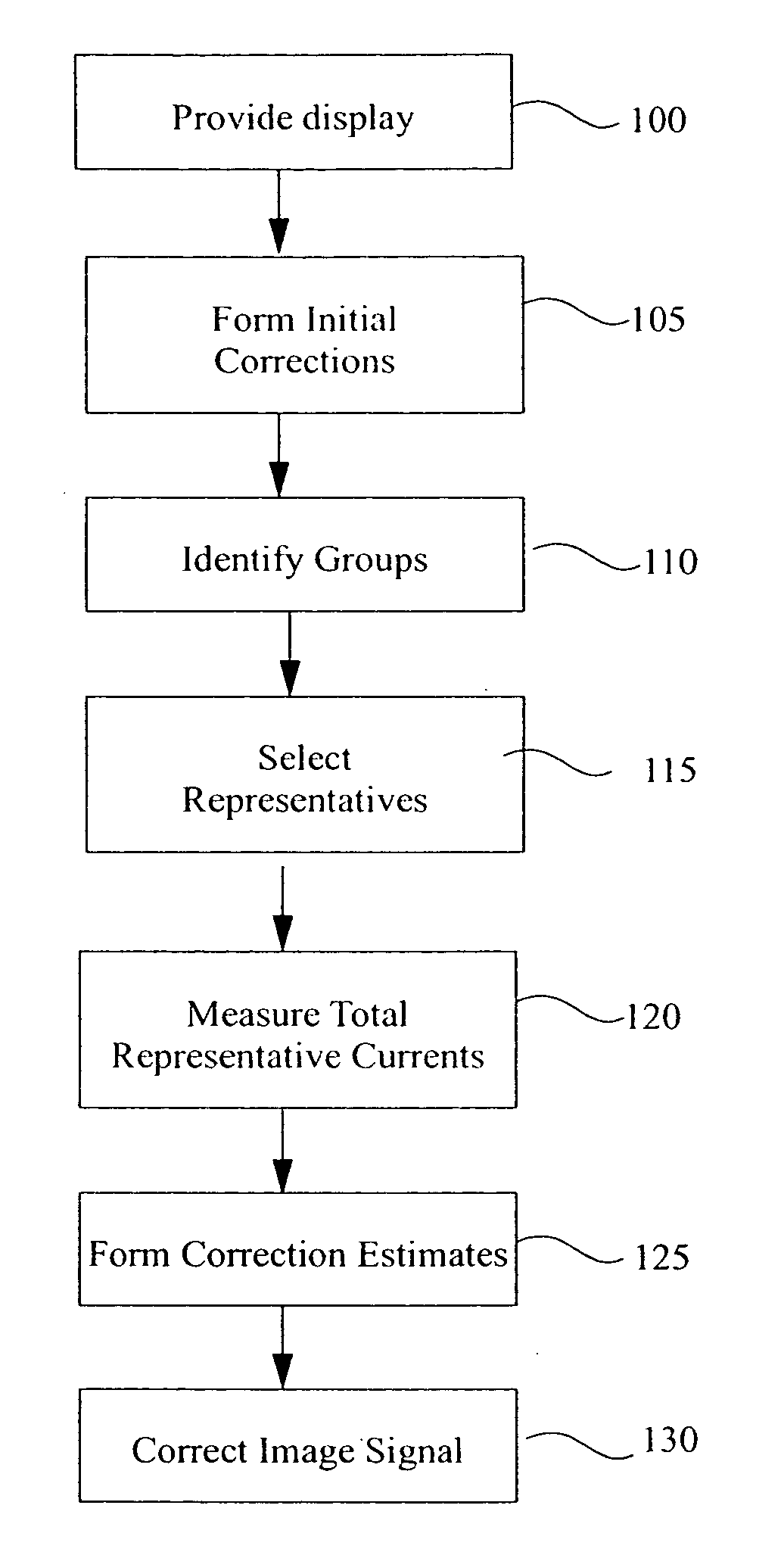
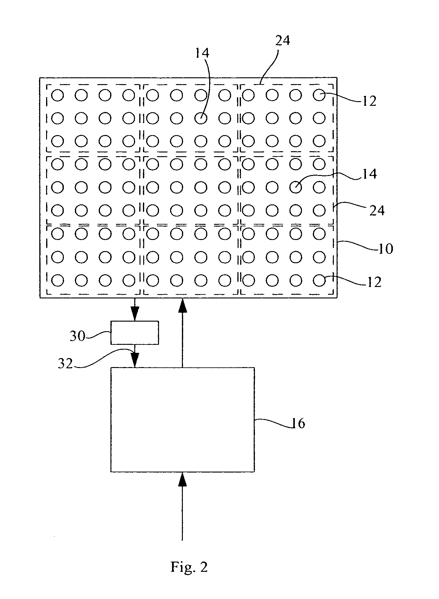
[0016]Referring to FIG. 1, a method for reducing brightness uniformity variations in an active-matrix OLED display employing amorphous silicon thin-film transistors is disclosed, comprising the steps of providing 100 an active-matrix OLED display having amorphous silicon thin-film transistors that drive a plurality of light-emitting elements responsive to an input signal that cause the light-emitting elements to emit light; forming 105 a first correction value for each of the light-emitting elements derived from a measured or estimated value of light-emitting element performance in response to known image signals at a first time; identifying 110 a plurality of predetermined groups of light-emitting elements, the plurality of predetermined light-emitting groups including all of the light-emitting elements in the OLED display, wherein each predetermined group of light-emitting elements includes more than one light-emitting element; selecting 115 one or more representative light-emitti...


PUM


Abstract

A method for reducing brightness uniformity variations in an active-matrix OLED display employing amorphous silicon thin-film transistors, by providing an active-matrix OLED display having amorphous silicon thin-film transistors; and deriving a first correction value from a measured or estimated value of light-emitting element performance. Subsequently groups of light-emitting elements are identified, whereupon one or more representative light-emitting elements are selected. Remaining steps include measuring total representative current used by the representative light-emitting elements for each predetermined group of light-emitting element; deriving an estimated second correction value from the first correction value, or the measured or estimated value of light-emitting element performance, and the measured total representative currents for each individual light-emitting elements; and employing the estimated second correction value to correct image signals for the changes in the output of the light-emitting elements and produce compensated image signals.

Description

FIELD OF THE INVENTION[0001]The present invention relates to active-matrix OLED displays employing amorphous silicon thin-film transistors and having a plurality of light-emitting elements and, more particularly to reducing brightness variations in the light-emitting elements in the display.BACKGROUND OF THE INVENTION[0002]Flat-panel display devices, for example plasma, liquid crystal and Organic Light Emitting Diode (OLED) displays have been known for some years and are widely used in electronic devices to display information and images. Such devices employ both active-matrix and passive-matrix control schemes and can employ a plurality of light-emitting elements. The light-emitting elements are typically arranged in two-dimensional arrays with a row and a column address for each light-emitting element and having a data value associated with each light-emitting element to emit light at a brightness corresponding to the associated data value.[0003]Typical large-format displays (e.g....

Claims


Application Information

Patent Timeline
Patent Type & Authority Applications(United States)
IPC IPC(8): G09G3/30
CPCG09G3/006G09G3/3225G09G2320/0233G09G2320/0693G09G2320/029G09G2320/041G09G2320/043G09G2320/0285G09G2340/10
Inventor COK, RONALD S.
Owner GLOBAL OLED TECH
Why Eureka
Try Eureka