Thin-Film Transistor and Display Device using Oxide Semiconductor

a thin film transistor and display device technology, applied in the direction of semiconductors, semiconductor devices, electrical appliances, etc., can solve the problems of difficult to achieve normal-off operation of tft, difficult to make electric conductivity small, and difficult to enlarge the on/off ratio of transistors, etc., to achieve good interface characteristics and produce thin film tft.

Active Publication Date: 2009-03-19
CANON KK
View PDF12 Cites 192 Cited by
  • Summary
  • Abstract
  • Description
  • Claims
  • Application Information

AI Technical Summary

Benefits of technology

[0013]In consequence of having advanced energetically research and developments with regard to a TFT using a transparent oxide semiconductor, the present inventors obtained the following finding which could solve the above-described problems by employing the following structure. Thus, it is the structure of using as the above-described gate insulating film an insulating film which is composed of amorphous silicon containing at least O and N, and has a distribution of oxygen concentration in a thickness direction so that the oxygen concentration is high in a side of an interface with an oxide semiconductor layer and the oxygen concentration decreases toward a gate electrode. By using such an insulating film, it is possible to produce stably a thin film TFT with good interface characteristics.

Problems solved by technology

Since oxygen defects can be generated easily and many carrier electrons are generated in a conductive transparent oxide containing ZnO as a main component, it is difficult to make electric conductivity small.
In consequence, it becomes difficult to enlarge an on / off ratio of a transistor.
Also in this case, even at the time of not applying the gate voltage, a large current flows between the source terminal and drain terminal, and hence, it is difficult to achieve a normally-off operation of a TFT.
Furthermore, it is not necessarily easy to enlarge the on / off ratio of a transistor.
Moreover, when an insulating layer has a two-layer structure of using an oxide (e.g., SiO2) on a semiconductor interface side and highly insulating SiNx or the like on a gate electrode side as disclosed in Japanese Patent Application Laid-Open No. 2002-076356, there were the following problems.
That is, there were problems that hysteresis of TFT characteristics was expanded and reproducibility of TFT characteristics was poor since an interface was constructed in the insulating layer to generate defects.
In addition, when a TFT was formed on a film at a low temperature and a bending test was performed, degradation of the TFT characteristics was found which was considered to be caused by interface defects generated in the insulating layer having the two-layer structure.
Then, it is usually difficult to make crystal orientation and polycrystal grain size uniform, and to improve stability and reliability.
In addition, since a portion where grain size changes exists in a thickness direction at an early stage its polycrystalline structure is easy to become ununiform.
Since an insulating film surface had surface morphology according to the grain size, there was a problem that an interface between a channel layer and a gate insulating film, or an interface between the gate insulating film and a gate electrode metal did not become flat.

Method used


Image

  • Thin-Film Transistor and Display Device using Oxide Semiconductor
  • Thin-Film Transistor and Display Device using Oxide Semiconductor
  • Thin-Film Transistor and Display Device using Oxide Semiconductor

Examples


example 1

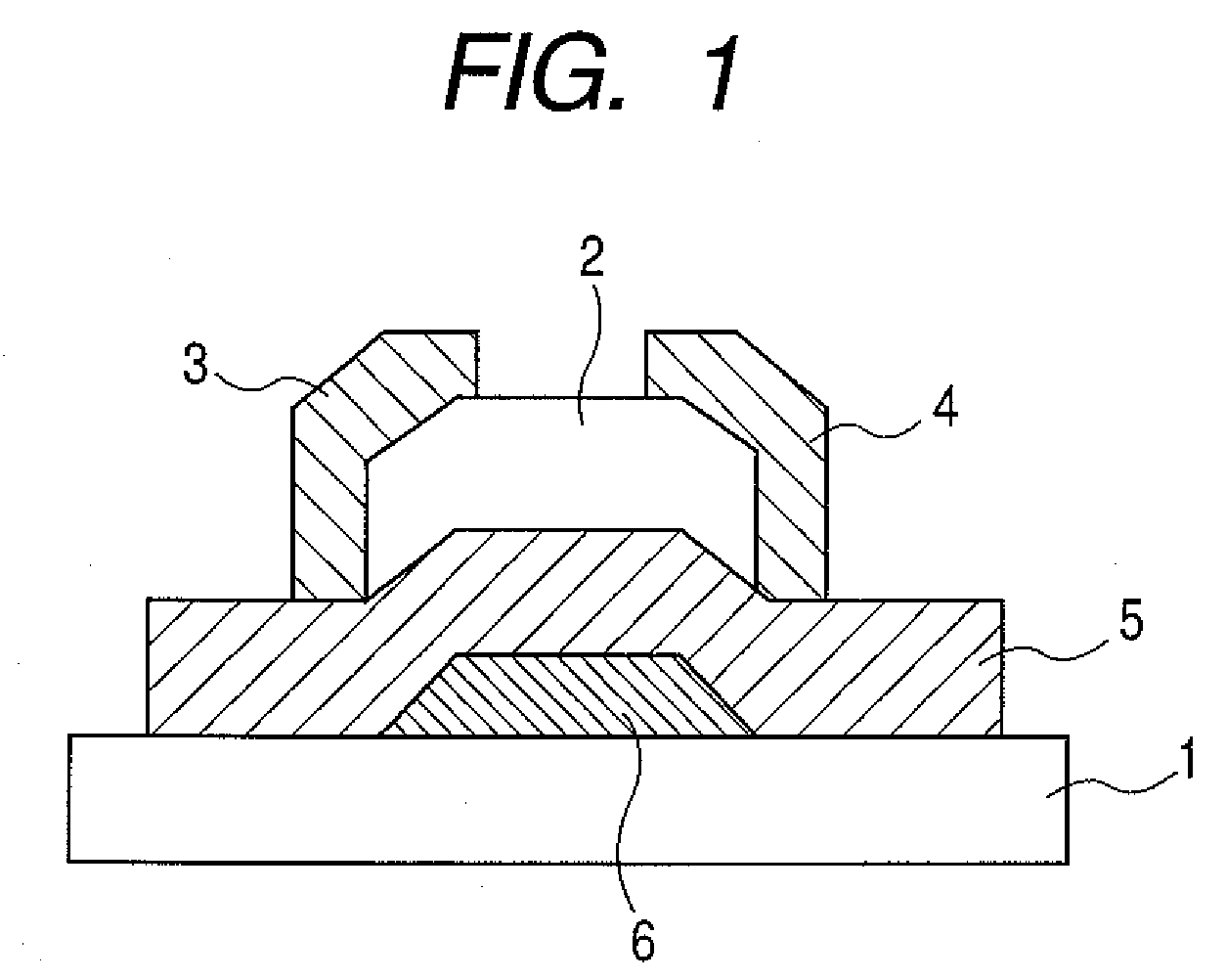
[0062]In this example, an inversed staggered (bottom gate type) MISFET element shown in FIG. 1 was produced so that an amorphous silicon oxynitride for forming a gate insulating film had a distribution of an oxygen concentration in a thickness direction thereof in which the oxygen concentration became high in the side of the interface with an oxide semiconductor. First of all, a gate terminal having a thickness of Ti:10 nm / Au:100 nm was formed on a glass substrate using a photolithographic method and a lift-off method. Furthermore, an insulating layer of a-SiOxNy was formed in a thickness of 100 nm thereon by a sputtering method. At that time, an Si2N3 target was used for a sputtering target and a mixed gas of Ar / O2 was used as a sputtering gas. The oxygen concentration of the mixed gas of Ar / O2 was changed to give the above distribution of an oxygen concentration to the insulating layer. Then, an amorphous oxide semiconductor film to be used as a channel layer was formed in a thick...

example 2

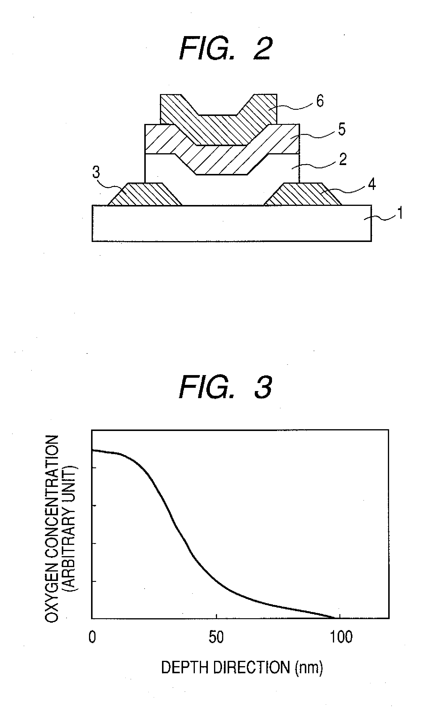
[0066]In this example, a staggered (top gate) type MISFET element as shown in FIG. 2 was produced. First, a film having a thickness of Ti:5-nm / Au:40-nm were stacked on a glass substrate 1, and a drain terminal 4 and a source terminal 3 were formed by a photolithographic method and a lift-off method. A 30 nm-thick amorphous In—Ga—Zn—O film having a metal composition ratio of In:Ga:Zn=1.00:0.94:0.65 which was used as a channel layer 2 was formed by a sputtering method. Furthermore, a 100 nm-thick insulating layer 5 of a-SiOxNy was formed thereon by the sputtering method. At that time, an Si2N3 target was used for a sputtering target and a mixed gas of Ar / O2 was used for a sputtering gas. The distribution of an oxygen concentration was given to an insulating layer by changing the oxygen concentration of the mixed gas of Ar / O2 so that the oxygen concentration of the insulating layer became high in the side of the interface with an oxide semiconductor. Moreover, a film having a thickness...

example 3

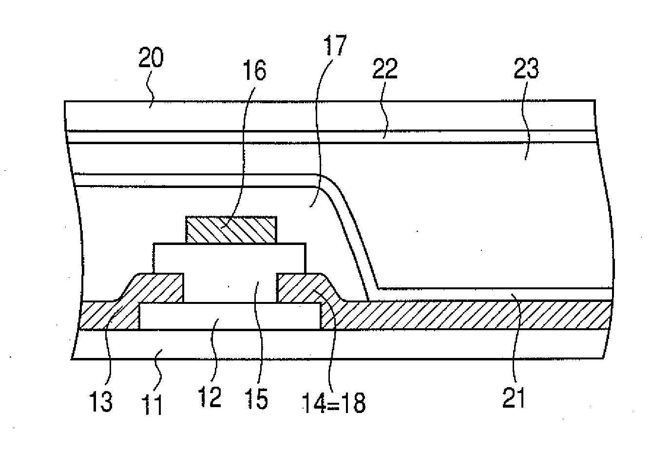
[0069]In this example, a display device using a TFT as shown in FIG. 7 will be explained. Production process of the TFT is the same as that in Example 2. In the above-described TFT, a short side of an island of an ITO film for forming a drain electrode is extended to 100 μm, the extended 90-μm portion is left, and after securing wiring to a source electrode and a gate electrode, the TFT is covered with an insulating layer. A polyimide film is coated thereon, and the resultant is subjected to a rubbing process. On the other hand, similarly, a plastic substrate having an ITO film and a polyimide film formed thereon and subjected to a rubbing process is prepared. This substrate is made to face the above prepared substrate having the above-described TFT formed thereon with an gap of 5 μm, and a nematic liquid crystal is injected to the gap. A pair of polarizing plates is further provided on both sides of this structure. Here, when a voltage is applied to the source electrode of the TFT ...


PUM


Abstract

The thin-film transistor of the present invention has at least a semiconductor layer including: on a substrate, a source electrode, a drain electrode, and a channel region; a gate insulating film; and a gate electrode, wherein the semiconductor layer is an oxide semiconductor layer, and wherein the gate insulating film is amorphous silicon including at least O and N, and the gate insulating film has a distribution of an oxygen concentration in a thickness direction so that the oxygen concentration is high in the side of an interface with an oxide semiconductor layer and the oxygen concentration decreases toward the side of the gate electrode.

Description

TECHNICAL FIELD[0001]The present invention relates to a thin-film transistor including amorphous silicon containing at least O and N as a gate insulating film; and a display device using the transistor.BACKGROUND ART[0002]Recently, as Japanese Patent Application Laid-Open No. 2002-076356 also discloses, developments of thin-film transistors (TFTs) each using a polycrystalline thin film of a transparent conductive oxide including ZnO as a main component for a channel layer have been actively performed.[0003]Since the above-mentioned thin film can be formed as a film at a low temperature and is transparent to visible light, and it is made possible to form a flexible transparent TFT on a substrates such as a plastic plate or a film.[0004]Furthermore, Japanese Patent Application Laid-Open No. 2003-086808 discloses that an insulating layer is formed into two-layer structure in a thin-film transistor which has a transparent semiconductor using ZnO or the like. Here, it is said that it is ...

Claims


Application Information

Patent Timeline
Patent Type & Authority Applications(United States)
IPC IPC(8): H01L29/786
CPCH01L21/28202H01L29/518H01L29/7869H01L21/02631H01L21/02554H01L21/02565H01L21/02422H01L29/4908H01L29/66969
Inventor HAYASHI, RYOABE, KATSUMISANO, MASAFUMI
Owner CANON KK
Why Eureka
Try Eureka