Systems and methods using sequential lateral solidification for producing single or polycrystalline silicon thin films at low temperatures

a technology of polycrystalline silicon and sequential solidification, applied in the direction of coatings, transistors, chemical vapor deposition coatings, etc., can solve the problems of poor and non-uniform devices, low manufacturing yield, and difficulty in achieving the effect of high-temperature solidification

Inactive Publication Date: 2003-06-03
THE TRUSTEES OF COLUMBIA UNIV IN THE CITY OF NEW YORK
View PDF15 Cites 183 Cited by
  • Summary
  • Abstract
  • Description
  • Claims
  • Application Information

AI Technical Summary

Problems solved by technology

The use of conventional excimer laser annealing technology to generate polycrystalline silicon is problematic for several reasons.
First, the polycrystalline silicon generated in the proce

Method used


Image

  • Systems and methods using sequential lateral solidification for producing single or polycrystalline silicon thin films at low temperatures
  • Systems and methods using sequential lateral solidification for producing single or polycrystalline silicon thin films at low temperatures
  • Systems and methods using sequential lateral solidification for producing single or polycrystalline silicon thin films at low temperatures

Examples


Embodiment Construction

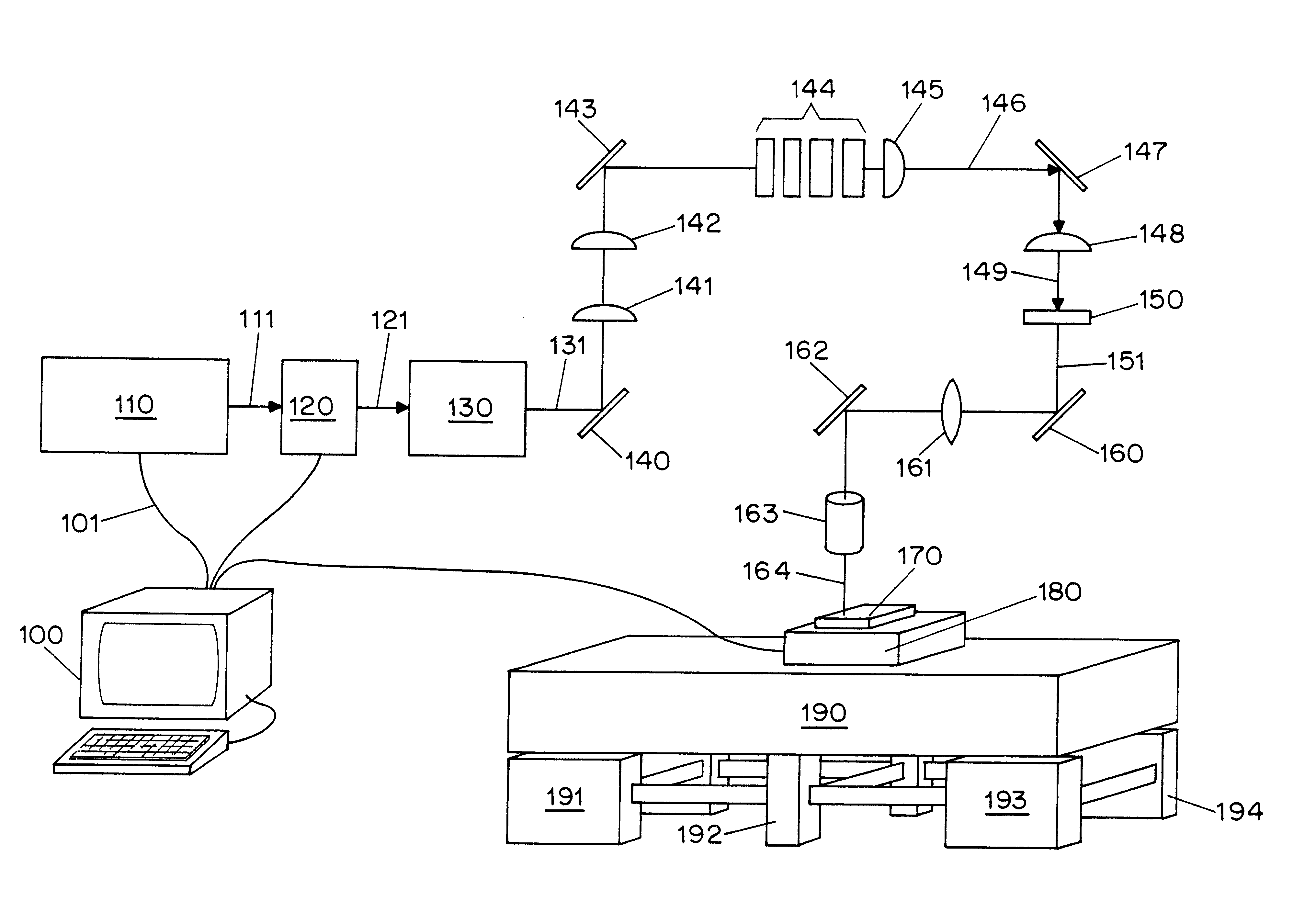
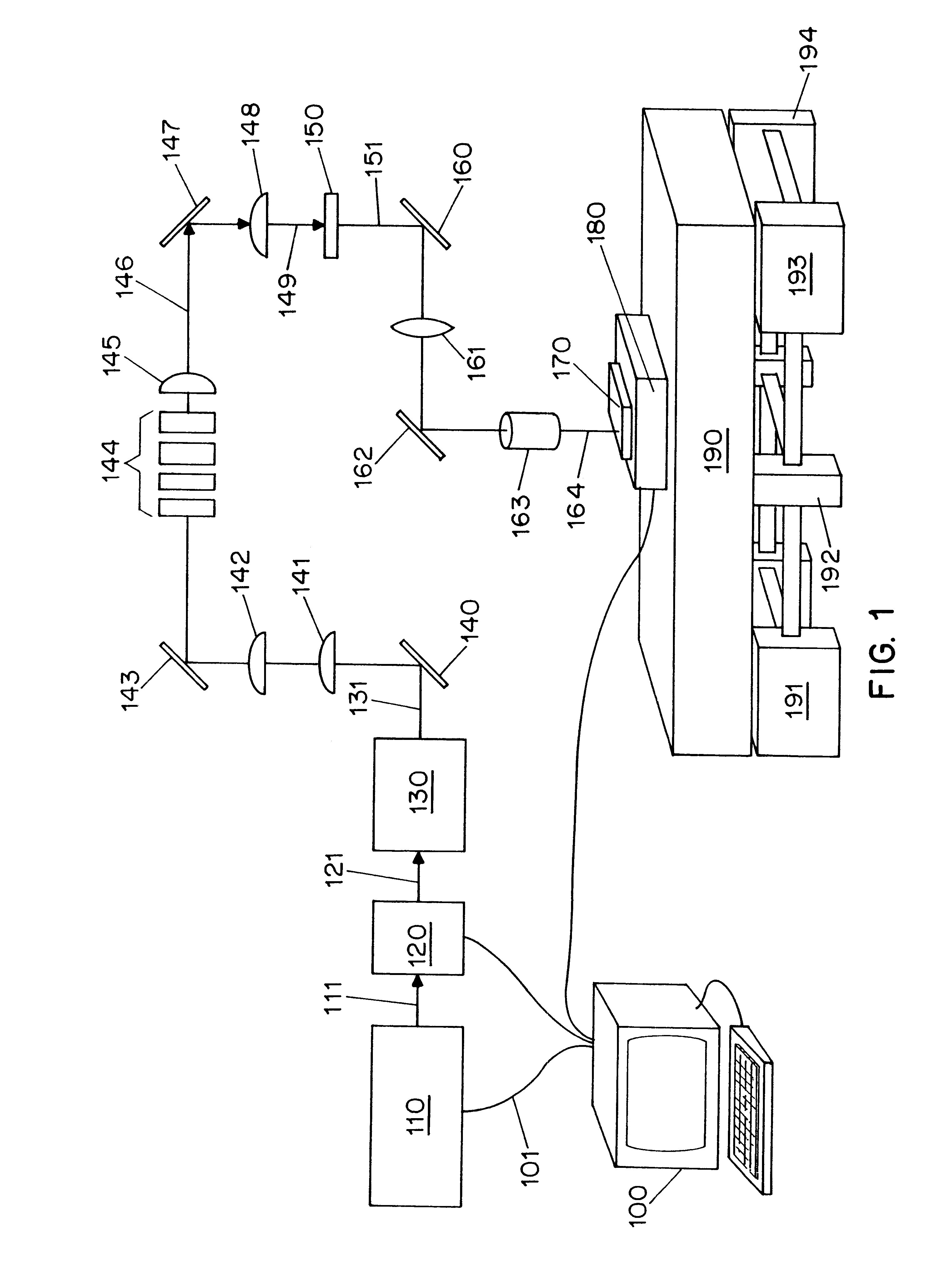
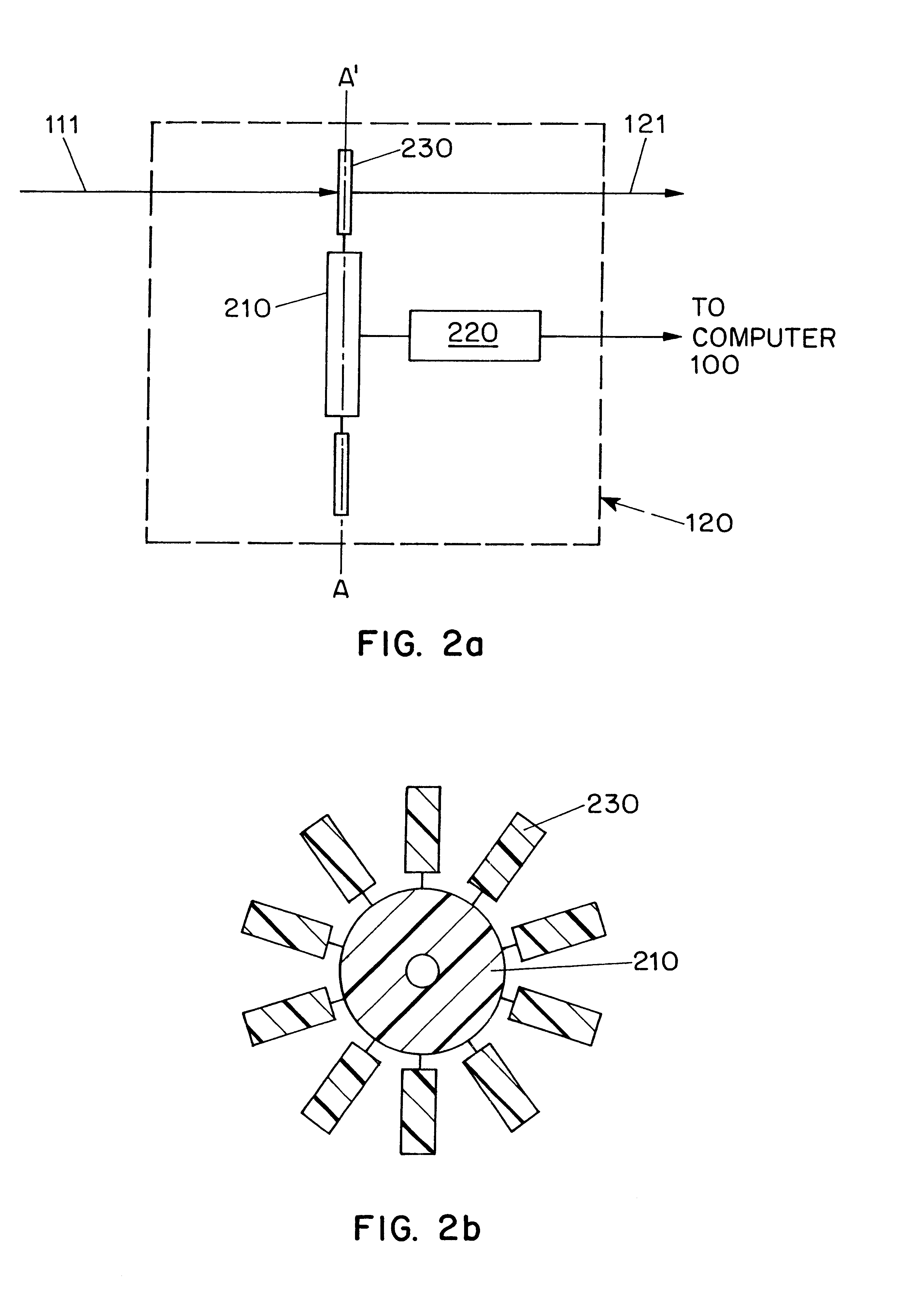
Referring to FIG. 1, a preferred embodiment of the present invention will be described. An excimer laser 110, which may be Lambda Physik Model LPX315i, generates a laser beam 110 which passes through an energy density modulator 120, described with greater particularity below. While the Lambda Physik excimer laser generates an ultraviolet beam at a wavelength of 308 nm, more powerful excimer lasers or excimer lasers generating beams at other wavelengths may be utilized. In accordance with the present invention, the modulator 120 acts to rapidly change the energy density of laser beam 110. The excimer laser 110 and energy density modulator 120 are each linked by a standard computer interface connection 101 to a computer 100 to effect control of the energy density modulator 120 in accordance with the timing of laser pulses generated by laser 110. The modulated laser beam 121 is directed through beam attenuator and shutter 130, which permit fine control over the fluence of the modulated...


PUM

PropertyMeasurementUnit
Attenuation coefficientaaaaaaaaaa
Energy densityaaaaaaaaaa

Abstract

System and methods for processing an amorphous silicon thin film sample into a single or polycrystalline silicon thin film are disclosed. The system includes an excimer laser for generating a plurality of excimer laser pulses of a predetermined fluence, an energy density modulator for controllably modulating fluence of the excimer laser pulses, a beam homoginizer for homoginizing modulated laser pulses in a predetermined plane, a mask for masking portions of the homoginized modulated laser pulses into patterned beamlets, a sample stage for receivingthe patterned beamlets to effect melting of portions of any amorphous silicon thin film sample placed thereon corresponding to the beamlets, translating means for controllably translating a relative position of the sample stage with respect to a position of the mask and a computer for controlling the controllable fluence modulation of the excimer laser pulses and the controllable relative positions of the sample stage and mask, and for coordinating excimer pulse generation and fluence modulation with the relative positions of the sample stage and mask, to thereby process amorphous silicon thin film sample into a single or polycrystalline silicon thin film by sequential translation of the sample stage relative to the mask and irradiation of the sample by patterned beamlets of varying fluence at corresponding sequential locations thereon.

Description

I. Field of the InventionThe present invention relates to techniques for semiconductor processing, and more particularly to semiconductor processing which may be performed at low temperatures.II. Description of the Related ArtIn the field of semiconductor processing, there have been several attempts to use lasers to convert thin amorphous silicon films into polycrystalline films. For example, in James Im et al., "Crystalline Si Films for Integrated Active-Matrix Liquid-Crystal Displays," 11 MRS Bullitin 39 (1996), an overview of conventional excimer laser annealing technology is presented. In such a system, an excimer laser beam is shaped into a long beam which is typically up to 30 cm long and 500 microns or greater in width. The shaped beam is scanned over a sample of amorphous silicon to facilitate melting thereof and the formation of polycrystalline silicon upon resolidification of the sample.The use of conventional excimer laser annealing technology to generate polycrystalline ...

Claims


Application Information

Patent Timeline
IPC IPC(8): H01L21/02H01L21/20C01B33/02H01L21/268
CPCH01L21/2026H01L21/02686H01L21/02678H01L21/02532H01L21/02595H01L21/02691H01L29/786
Inventor IM, JAMES S.SPOSILI, ROBERT S.CROWDER, MARK A.
Owner THE TRUSTEES OF COLUMBIA UNIV IN THE CITY OF NEW YORK
Why Eureka
Try Eureka