Organic luminescent display and manufacturing method thereof

A technology of light-emitting display and manufacturing method, which is applied in semiconductor/solid-state device manufacturing, electroluminescence light source, light source, etc., and can solve problems such as difficulty in controlling the optimal width of the gap, breaking of the sealant layer, and too wide a gap reserved

Active Publication Date: 2008-02-13
AU OPTRONICS CORP
View PDF4 Cites 0 Cited by
  • Summary
  • Abstract
  • Description
  • Claims
  • Application Information

AI Technical Summary

Problems solved by technology

When the substrates are pressed together, as shown in Figure 1c, due to the increase in the internal gas pressure, it is easy to cause the width of the sealant layer at the joint 14 to be too large, resulting in the overflow of the sealant
[0006] Or reserve a wider gap on the path covering the sealant layer (non-corner position) whose starting point and end point will not extend to the outside to release gas. Although it is more conducive to the discharge of gas, the diffusion path of the sealant layer is still Affected by the released gas, it is difficult to control the optimal width of the gap, and there is a problem that the gap is too wide or too narrow. If the gap is too wide, the width of the joint of the sealant layer may be insufficient, or even appear. If the joint cannot be joined, if the reserved gap is too small, the sealant layer will often be broken due to the sudden increase of internal pressure

Method used


Image

  • Organic luminescent display and manufacturing method thereof
  • Organic luminescent display and manufacturing method thereof
  • Organic luminescent display and manufacturing method thereof

Examples


Embodiment

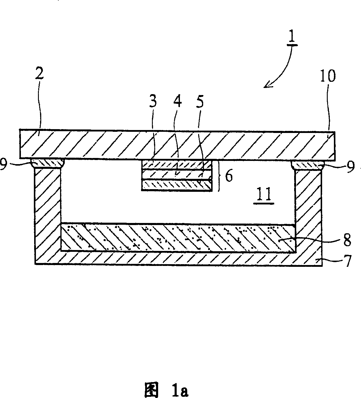
[0045] Please refer to FIG. 2 , illustrating an embodiment of the present invention, the fabrication of an organic light emitting display. First, as shown in FIG. 2 , a substrate 22 is provided. The substrate 22 is a light-transmitting glass, polymer, ceramic or plastic substrate, wherein the plastic substrate is made of polyethylene terephthalate (polyethyleneterephthalate), polyester (polyester), polycarbonate (polycarbonates), polyacetamide ( polyimide), Arton, polyacrylates (polyacrylates) or polystyrene (polystyrene) materials.

[0046] Next, a first electrode 25 is formed on the substrate 22 . The first electrode 25 is, for example, a transparent electrode, or an anode conductive layer, and the transparent electrode is indium tin oxide (ITO), indium zinc oxide (IZO), zinc aluminum oxide (AZO) or zinc oxide (ZnO ).

[0047] Continuing to form an organic light-emitting structure layer on the first electrode 25, the organic light-emitting structure layer sequentially inc...


PUM


Abstract

The invention discloses a organic light display, it includes: a basal plate, a glue layer, which is formed on the frame of the basal plate, there is at least one corner of the frame has a gap. The invention also includes the producing method of the organic light display.

Description

technical field [0001] The invention relates to a photoelectric device, in particular to an organic light-emitting display and a manufacturing method thereof. Background technique [0002] Generally speaking, after long-term use of organic light-emitting displays, moisture in the environment can easily penetrate into the display through the interface between the back cover and the substrate. Since the component electrodes are usually made of highly active metals, the It reacts with the water vapor infiltrated into the display, and the structure of the metal layer itself is relatively loose, and the water vapor will affect the light-emitting elements of the lower layer through this path, causing phenomena including peeling or material cracking between the metal electrode and the organic light-emitting layer , leading to the generation of dark spots, greatly reducing the luminous intensity and uniformity of the organic light-emitting display, and reducing the life of the devic...

Claims


Application Information

Patent Timeline
Patent Type & Authority Patents(China)
IPC IPC(8): H01L51/52H01L51/56H05B33/04H05B33/10H05B33/12
Inventor 施国辉
Owner AU OPTRONICS CORP
Why Eureka
Try Eureka