


Quick Research
Generate reliable direction feasibility study reports for your R&D in just a few steps.

Technical Q&A
Discover and master advanced knowledge NOW. Basics, ideas, possibilities, all at once.

Find Solutions
As an expert in R&D theories, this can generate solutions to your technical problems instantly.

Evaluate Feasibility
Analyze your overall solution with one click, know your potential R&D risks in advance.

Monitor Landscape
Get weekly tech updates, stay abreast of the latest tech innovations and key insights.
Two layer LTO backside seal for a wafer
A wafer and backside technology, applied in the process field of low temperature oxide deposition
- Summary
- Abstract
- Description
- Claims
- Application Information
AI Technical Summary
Problems solved by technology
Method used
Image

Examples
Embodiment Construction
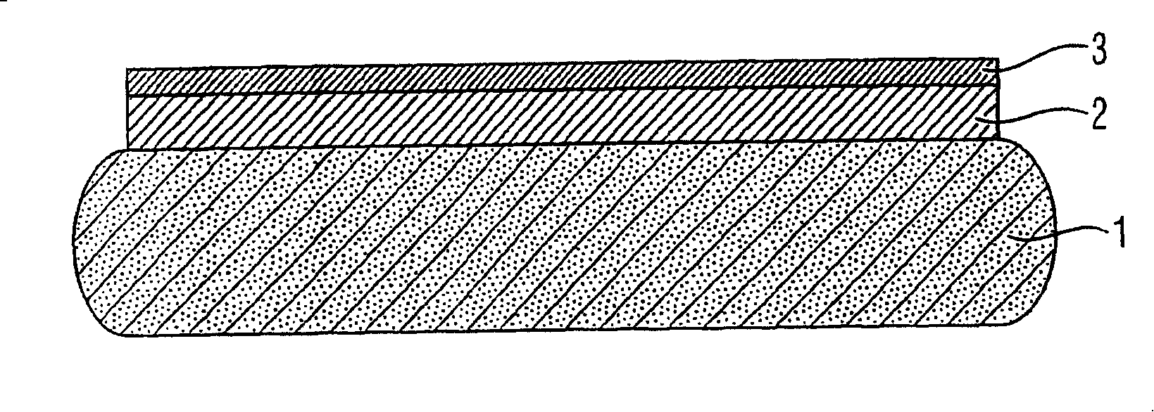
[0013] figure 1 Denotes a silicon wafer with two LTO layers forming a backside seal. The substrate 1 is doped (p-type or n-type) silicon. Layer 2 is made using high silane (SiH 4 ) flow using high frequency RF at high power to form a low stress LTO layer. Layer 3 is deposited on layer 2 using high and low frequency RF at high power, thereby providing a high density high stress LTO layer which has a lower etch rate during the subsequent cleaning process.
[0014] The low stress LTO layer 2 controls the geometry of the wafer to minimize warpage of the wafer. This low stress LTO layer also serves to improve edge blurring during epitaxy.
[0015] The high stress LTO layer has a high density and thus a low etch rate. This allows the backside seal to maintain the low stress LTO layer during the subsequent cleaning process since only a small amount of the highly stressed LTO layer is available for etching. The low stress LTO layer also has a high deposition rate, which means a ...
PUM
 Abstract
Description
Claims
Application Information
 - R&D Engineer
- R&D Manager
- IP Professional
- Industry Leading Data Capabilities
- Powerful AI technology
- Patent DNA Extraction
Browse by: Latest US Patents, China's latest patents, Technical Efficacy Thesaurus, Application Domain, Technology Topic, Popular Technical Reports.
© 2024 PatSnap. All rights reserved.Legal|Privacy policy|Modern Slavery Act Transparency Statement|Sitemap|About US| Contact US: help@patsnap.com