Method for generating a structure on a substrate

一种基板、氮化层的技术,应用在电气元件、半导体/固态器件制造、电路等方向,能够解决艰难具有可能性、无法达到栅极长度、短栅极结构不可能等问题

Inactive Publication Date: 2009-04-08
INFINEON TECH AG
View PDF7 Cites 0 Cited by
  • Summary
  • Abstract
  • Description
  • Claims
  • Application Information

AI Technical Summary

Problems solved by technology

[0003] In the state of the art, lithography methods are known and (multiple) gate electrodes can be fabricated by using these lithography methods, and since these known methods are not self-explanatory Alignment, therefore, will cause restrictions based on the limited alignment possibilities of the used lighting equipment, and moreover, the disadvantage of the grid structure produced is that it may not be possible to achieve a specific gate length, and may not be able to achieve specific tolerances
[0004] Furthermore, a further disadvantage of the known methods is that a different doping of the source region and the drain region, as it is required in, for example, an LDMOS transistor, or a DMOS transistor Similarly, the system is only difficultly possible, or, for short gate structures, it is not possible at all

Method used


Image

  • Method for generating a structure on a substrate
  • Method for generating a structure on a substrate
  • Method for generating a structure on a substrate

Examples


Embodiment Construction

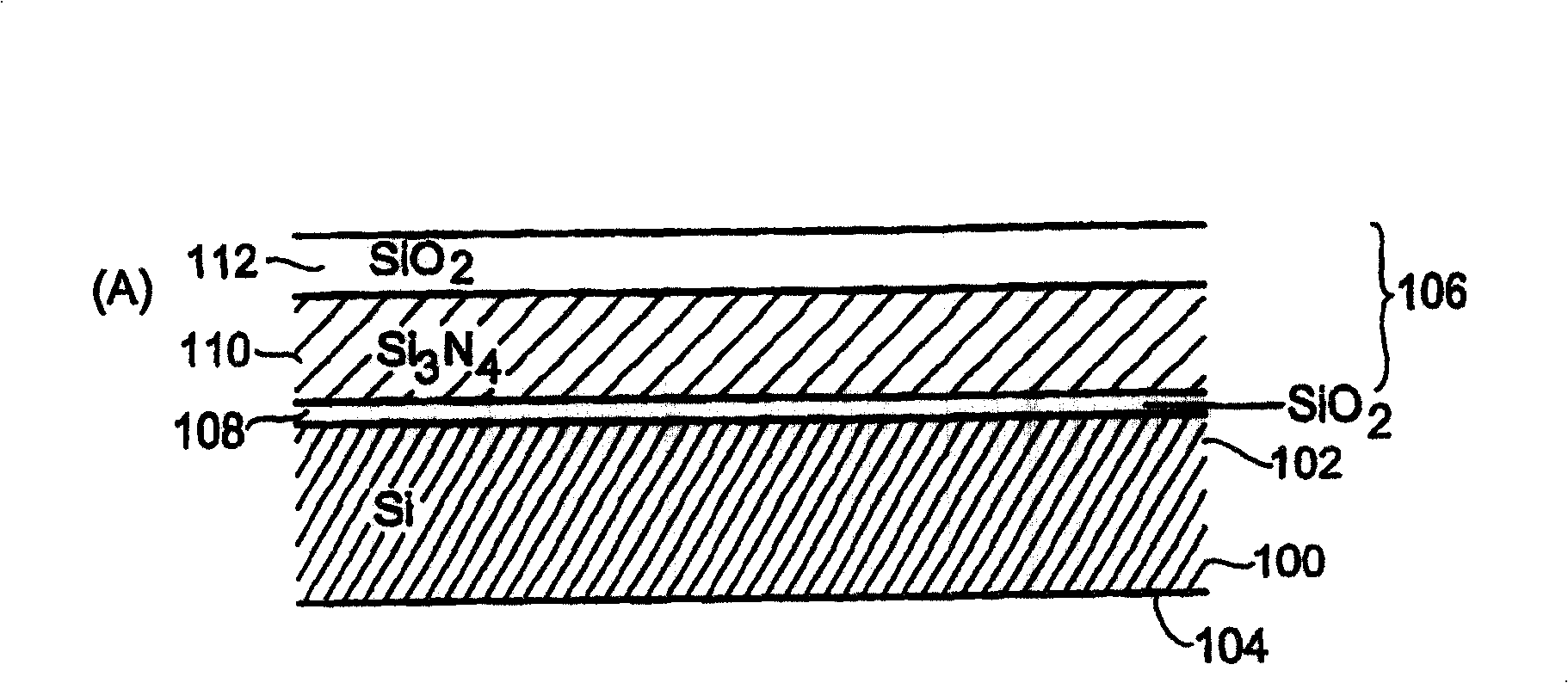
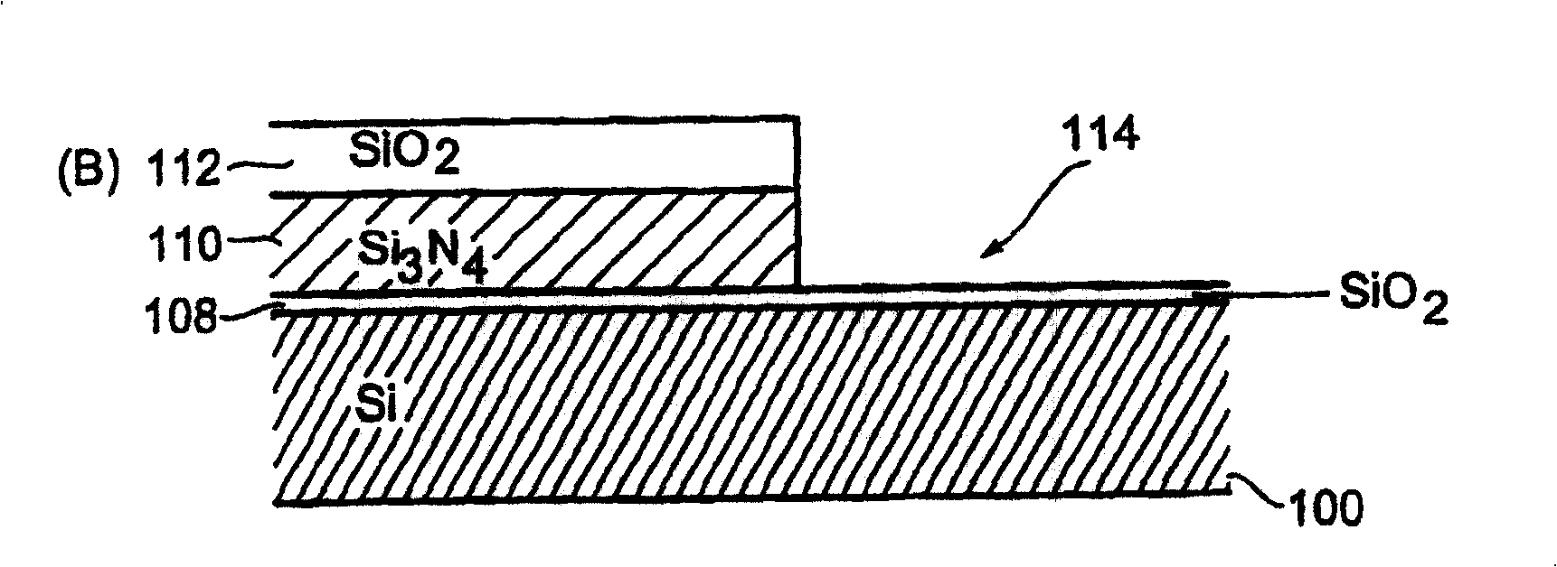
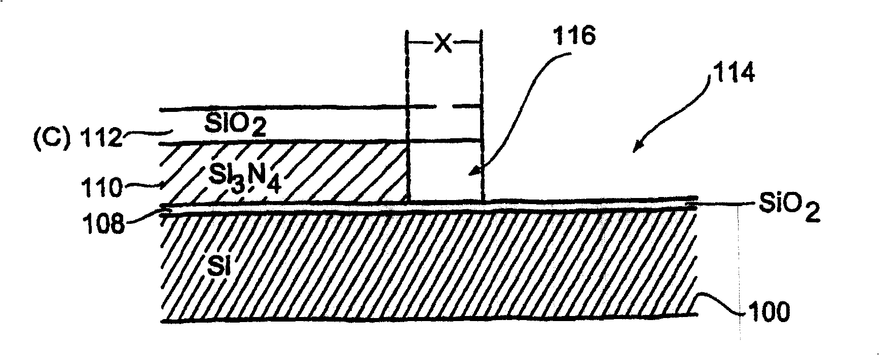
[0021] Now, referring to Fig. 1, a first preferred embodiment of the present invention will be explained in more detail, wherein, using Figure 1A to Figure 1K , the different program steps according to this preferred embodiment will be explained in more detail.

[0022] exist Figure 1A In, a semiconductor structure is illustrated, which includes a substrate 100 having a first major surface 102 and a second major surface 104, and in the illustrated embodiment is a silicon substrate On the first major surface 102 of the substrate 100, a layer sequence 106 is produced, including a first oxide layer 108 disposed on the substrate 100, a first oxide layer 108 disposed on the first oxide layer 108 Nitride layer 110, and a second oxide layer 112 disposed on the nitride layer 110, moreover, in the illustrated embodiment, these oxide layers 108 and 112 are silicon dioxide layers, and The nitride layer 110 is a silicon nitride layer, and, in Figure 1A The silicon oxide / silicon nitri...


PUM

PropertyMeasurementUnit
etching rateaaaaaaaaaa
lengthaaaaaaaaaa

Abstract

Disclosed is a method for creating a structure(132)on a substrate (100), according to which a first oxide layer, a first nitride layer, and a second oxide layer are successively applied to the substrate (100) in a first step. A section of the second oxide layer and a section of the first nitride layer are then removed in order to expose a section of the first oxide layer. A portion of the first nitride layer, which is located on top of the first oxide layer and below the second oxide layer(112), is subsequently removed in order to define the area of the structure(132).

Description

technical field [0001] The present invention relates to a method of producing a structure on a substrate and, in particular, to a self-aligning Standard (self-aligning) method. Background technique [0002] In some applications for manufacturing semiconductors, it may be necessary to implement structures with smaller (shorter) dimensions, for example, in MOS transistors (MOS=metal oxide semiconductor), for example, in LDMOS transistors ( LDMOS=laterally diffused metal oxide semiconductor, laterally diffused metal oxide semiconductor), gate electrode, or gate oxide, among them. [0003] In the state of the art, lithography methods are known and (multiple) gate electrodes can be fabricated by using these lithography methods, and since these known methods are not self-explanatory Alignment, therefore, will cause restrictions based on the limited alignment possibilities of the used lighting equipment, and moreover, the disadvantage of the grid structure produced is that it may...

Claims


Application Information

Patent Timeline
Patent Type & Authority Patents(China)
IPC IPC(8): H01L21/336H01L21/28H01L21/311H01L21/8242
CPCH01L21/2815
Inventor C·赫祖姆
Owner INFINEON TECH AG
Why Eureka
Try Eureka