A method for manufacturing a T-shaped gate of a high electron mobility transistor

A technology with high electron mobility and manufacturing methods, applied in semiconductor/solid-state device manufacturing, circuits, electrical components, etc., can solve the problems of high MMIC yield, unobtainable, unreachable, etc.

Active Publication Date: 2020-07-07
CHENGDU HIWAFER SEMICON CO LTD
View PDF7 Cites 0 Cited by
  • Summary
  • Abstract
  • Description
  • Claims
  • Application Information

AI Technical Summary

Problems solved by technology

[0003] At present, thermal deformation is usually used to manufacture the lower root cavity with rounded corners in the manufacture of T-shaped gates, but thermal deformation cannot obtain a sufficiently small gate length, and cannot achieve a high MMIC yield.

Method used


Image

  • A method for manufacturing a T-shaped gate of a high electron mobility transistor
  • A method for manufacturing a T-shaped gate of a high electron mobility transistor
  • A method for manufacturing a T-shaped gate of a high electron mobility transistor

Examples


Embodiment Construction

[0020] In order to make the purpose, technical solution and advantages of the present application clearer, the present application will be further described in detail below in conjunction with the accompanying drawings and specific embodiments. For simplicity, some technical features known to those skilled in the art are omitted from the following description.

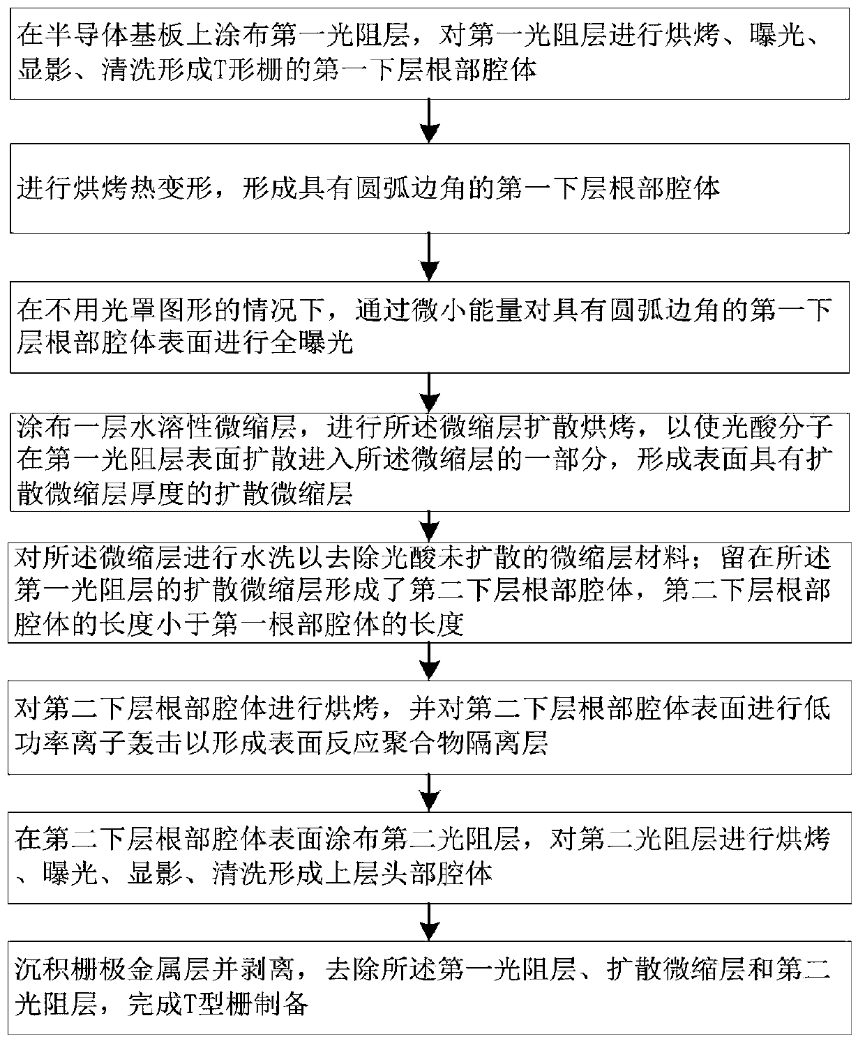
[0021] Such as figure 1 As shown, this embodiment provides a method for manufacturing a T-shaped gate of a high electron mobility transistor, comprising the following steps:

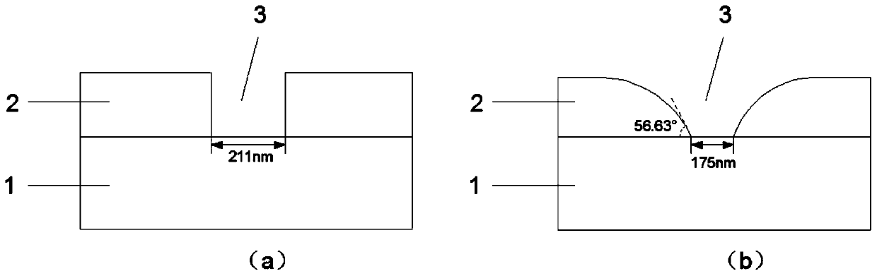
[0022] S1. Coating the first photoresist layer 2 on the semiconductor substrate 1, baking, exposing, developing and cleaning the first photoresist layer 2 to form the first lower root cavity 3 of the T-shaped grid, as figure 2 As shown in a, the length of the root cavity 3 of the first lower layer is 211 nm at this time;

[0023] S2. Perform baking thermal deformation to form the first lower root cavity 3 with arc corners, such as figure 2 A...


PUM

PropertyMeasurementUnit
wavelengthaaaaaaaaaa
lengthaaaaaaaaaa

Abstract

The invention relates to the technical field of semiconductor manufacturing, and specifically relates to a manufacturing method of T-shaped gate of a high electron mobility transistor. The manufacturing method includes the following steps: S1, coating a first photoresist layer on a semiconductor substrate, and forming a first lower layer of root cavity; S2, performing baking and thermal deformation to form a first lower layer of root cavity with an arc corner; S3, performing total exposure on the surface of the first lower layer of root cavity; S4, coating a water-soluble micro-shrink layer, and performing diffused baking on the micro-shrink layer to form a diffused micro-shrink layer with the diffused micro-shrink layer thickness; S5, washing to remove the micro-shrink layer material on which the photoacid is not removed to form a second lower layer of root cavity; S6, performing low power ion bombardment to form a surface reaction Polymer separating layer; S7, forming an upper layerof head cavity; and S8, depositing and peeling a gate metal layer. The manufacturing method of T-shaped gate of a high electron mobility transistor can further reduce the gate length of the T-shaped gate through the steps of heat deformation, total exposure, diffusion of the micro-shrink layer, and low power ion bombardment.

Description

technical field [0001] The invention belongs to the technical field of semiconductor manufacturing, and in particular relates to a method for manufacturing a T-shaped gate of a high electron mobility transistor. Background technique [0002] For HEMT devices in MMICs, the maximum operating frequency f max is the frequency at which the gain decreases to 1, which is mainly determined by the gate length, transconductance and die parasitic parameters (such as gate resistance Rg, capacitance C). The HEMT gate length required by the commonly used Ka-band MMICs is 0.15 microns, which will lead to a severe reduction in the cross-section, resulting in a rapid increase in the gate resistance Rg, which severely limits the maximum operating frequency f of the transistor max , and affects the reliability of the gate at high output power and high leakage current. In order to ensure high operating frequency and high reliability of HEMT devices, T-shaped gates with short gate length, larg...

Claims


Application Information

Patent Timeline
Patent Type & Authority Patents(China)
IPC IPC(8): H01L21/285
CPCH01L21/28587
Inventor 闫未霞
Owner CHENGDU HIWAFER SEMICON CO LTD
Why Eureka
Try Eureka