A kind of power semiconductor device and its manufacturing method

A technology for power semiconductors and semiconductors, applied in the manufacture of semiconductor/solid-state devices, semiconductor devices, electrical components, etc., can solve the problems of increasing on-resistance, limiting the performance of the split gate VDMOS, limiting the value of the device, etc., to reduce the electric field strength, Optimized switching performance, effect of small gate length

Inactive Publication Date: 2020-11-27
UNIV OF ELECTRONICS SCI & TECH OF CHINA
View PDF4 Cites 0 Cited by
  • Summary
  • Abstract
  • Description
  • Claims
  • Application Information

AI Technical Summary

Problems solved by technology

However, the introduced split gate structure also reduces the open gate accumulation area, increases the on-resistance, and limits the device figure of merit
In addition, the additional gate-source capacitance introduced by the grounded split gate also limits the performance of the split gate VDMOS

Method used


Image

  • A kind of power semiconductor device and its manufacturing method
  • A kind of power semiconductor device and its manufacturing method
  • A kind of power semiconductor device and its manufacturing method

Examples


Embodiment 1

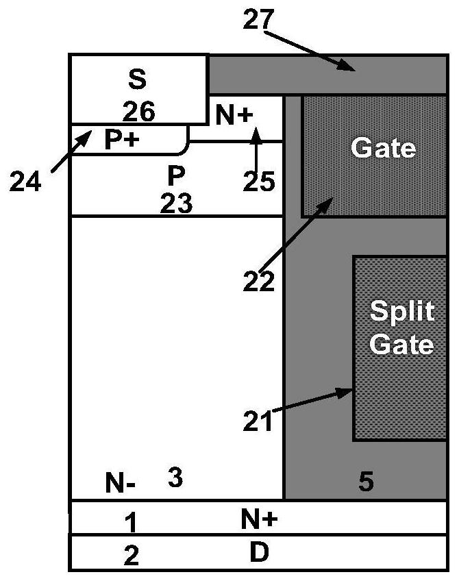
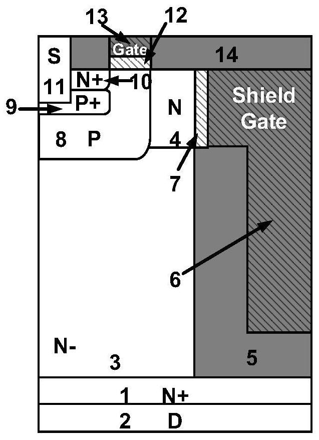
[0041] Such as figure 2As shown, a power semiconductor device includes a first conductivity type semiconductor substrate 1, the bottom of the first conductivity type semiconductor substrate 1 is connected to the drain electrode 2; the upper part of the first conductivity type semiconductor substrate 1 has a first Conductive type semiconductor epitaxial layer 3; the first conductive type semiconductor epitaxial layer 3 has a dielectric groove 5, and the dielectric groove 5 has an isolation gate 6; the upper part of the first conductive type semiconductor epitaxial layer 3 has a second conductive type semiconductor body Region 8, the second conductivity type semiconductor body region 8 has a second conductivity type semiconductor body contact region 9 and a first conductivity type semiconductor source region 10; the second conductivity type semiconductor body contact region 9 and the first conductivity type The semiconductor source regions 10 are all connected to the source ele...

Embodiment 2

[0065] The difference between this embodiment and Embodiment 1 is that the potential of the isolation barrier 6 is not grounded, but connected to a specific potential, which can be provided by other parts of the circuit. All the other structures are the same as in Example 1.

[0066] According to the common knowledge in this field, it can be known that connecting a specific voltage can modulate the electric field distribution in the body, increase the breakdown voltage, and reduce the on-resistance, or connect a point voltage signal or other dynamic voltage that changes synchronously with the gate voltage, which can further increase the switching speed or ratio on-resistance for better device performance.

Embodiment 3

[0068] Such as Figure 4 As shown, the difference between this embodiment and Embodiment 1 is that the medium in the dielectric tank 5 adopts a multilayer variable permittivity structure, including a first dielectric layer 15 with a dielectric constant of K1 and a first dielectric layer 15 with a dielectric constant of K2. Two dielectric layers 16 . All the other structures are the same as in Example 1. In this embodiment, the dielectric constants of the first dielectric layer 15 and the second dielectric layer 16 are optimized, so as to modulate the electric field in the device and introduce a new electric field peak, which can effectively increase the breakdown voltage of the device and further improve the device's performance. The excellent values ​​of breakdown voltage and on-resistance improve the overall performance of the device.


PUM


Abstract

The present invention proposes a power semiconductor device with a junction barrier region and a short lateral channel and its manufacturing method, through the body region and the isolation gate, the junction barrier region is quickly depleted at a lower drain voltage to form a depletion layer , block the capacitive coupling between the gate and drain, and at the same time use the lateral channel and vertical junction barrier regions to reduce the electric field strength of the gate-channel boundary PN junction in the off state, suppress the occurrence of punch-through, and achieve smaller The length of the gate reduces the Miller capacitance, reduces the dynamic loss caused by the gate switch, and optimizes the switching performance of the device. In addition, the groove-shaped isolation gate assists in depleting the drift region and increases the doping concentration of the drift region to achieve a lower on-resistance.

Description

technical field [0001] The invention relates to the technical field of semiconductor devices, and relates to a power semiconductor device with optimized switching performance and a manufacturing method thereof. Background technique [0002] The power semiconductor device is an essential core device to realize electric energy conversion and control, and is a bridge for weak current to control strong current. Low-voltage VDMOS (12V–250V) is widely used in circuits such as DC transformers and three-phase inverters. In order to reduce power consumption and improve device efficiency, the RESURF stepped oxide layer (RSO) structure proposed in other patents ( US7372103B2) or super junction technology (US5216275A) to achieve lower specific on-resistance. However, with the continuous improvement of the operating frequency of modern power systems, the proportion of dynamic losses caused by the switching process of devices is increasing, which greatly affects the switching performance...

Claims


Application Information

Patent Timeline
Patent Type & Authority Patents(China)
IPC IPC(8): H01L29/78H01L29/423H01L21/336
CPCH01L29/7802H01L29/7813H01L29/4236H01L29/66734H01L29/407H01L29/0878H01L29/66712
Inventor 周锌王睿迪李治璇王正康乔明李肇基张波
Owner UNIV OF ELECTRONICS SCI & TECH OF CHINA
Why Eureka
Try Eureka