Fast recovery diode FRD chip and production process for same

A technology for recovering diodes and chips, used in semiconductor/solid-state device manufacturing, electrical components, circuits, etc., can solve the problems of uneven redistribution of metal ions, uneven distribution of metal ions, uneven reverse recovery time, etc. Enhanced voltage stability and reliability, improved flatness, uniform and stable reverse recovery time

Active Publication Date: 2014-12-10
SUZHOU QILAN POWER ELECTRONICS
View PDF12 Cites 24 Cited by
  • Summary
  • Abstract
  • Description
  • Claims
  • Application Information

AI Technical Summary

Problems solved by technology

[0002] At present, the production of fast recovery diode (FRD) chips in the semiconductor industry usually adopts the phosphorus-boron paper source diffusion process or the epitaxial wafer substrate boron diffusion process. The breakdown voltage is not stable enough, and the anti-surge ability is poor; 2) The forward voltage drop is large, and the power consumption is large; 3) The concentration of the paper source is too high to absorb doped metal ions, which makes the distribution of metal ions uneven, resulting in reverse recovery The time is not uniform, and the leakage current increases at the same time; 4) The cost of the epitaxial wafer is high, and the doping concentration of the epitaxial layer is high, which will also lead to discrete recovery time; 5) The melting temperature of glass powder used in glass passivation in the industry is 800 ° C ~ 850°C, so a high glass firing temperature should be used, which will also cause uneven redistribution of metal ions, abnormal recovery time, and poor switching characteristics

Method used


Image

  • Fast recovery diode FRD chip and production process for same
  • Fast recovery diode FRD chip and production process for same
  • Fast recovery diode FRD chip and production process for same

Examples


Embodiment Construction

[0033] A fast recovery diode FRD chip and its manufacturing process according to the present invention will be further described in detail through specific embodiments below.

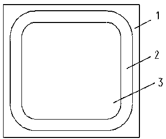
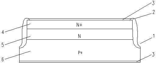
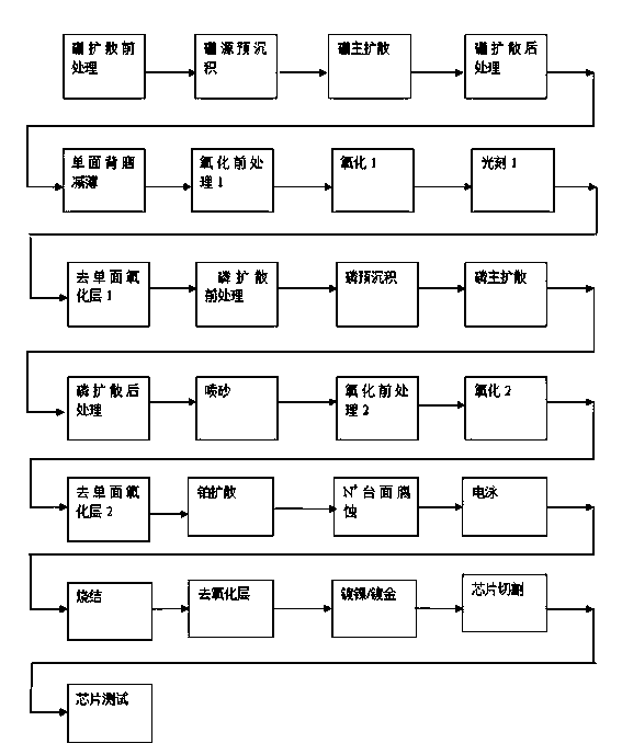
[0034] A kind of production technology of fast recovery diode FRD chip, see image 3 , which has the following steps:

[0035] 1) Pre-diffusion treatment: through electronic cleaning agent SC 2 , Ultrasonic cleaning with deionized water and other processes to chemically treat the surface of the silicon wafer to obtain a clean original N-type silicon wafer;

[0036] 2) Boron source pre-deposition: pre-deposit the cleaned original N-type silicon wafer in a diffusion furnace at 1150-1200 ° C with gas carrying into a liquid boron source (boron tribromide);

[0037] 3) Main diffusion of boron source: carry out deep junction diffusion on the pre-deposited silicon wafer in a diffusion furnace at 1200-1250°C to form a deep P + Floor;

[0038] 4) Post-diffusion treatment: Soak in hydrofluoric acid and ultras...


PUM


Abstract

The invention relates to a fast recovery diode FRD chip and a production process for the same. The process comprises the following steps of: diffusion pre-treatment, boron source pre-deposition, boron source main diffusion, diffusion after-treatment, single-surface back grinding thinning, oxidation pre-treatment, oxidation, photoetching, single-surface oxide layer removal, phosphorus source pre-deposition, phosphorus diffusion, sand blasting, platinum diffusion, N + surface mesa etching, electrophoresis, sintering, oxide layer removal, nickel plating, gold plating and chip cutting, wherein the structure of the obtained chip is P+-N-N+ type. According to the process, the uniformity of the reverse recovery time of the fast recovery diode is improved and controllability is improved, meanwhile, voltage drop is reduced, leakage current is reduced, and voltage-proof stability is improved; the contradiction of mutual condition among the reverse voltage, the positive voltage, the reverse recovery time and the leakage current of the fast recovery diode is solved to enable the various parameters to achieve the optimal matching, thus improving the reliability and switching characteristic of the diode, and reducing power consumption. The fast recovery diode disclosed by the invention breaks through the technical bottleneck of the traditional fast recovery diodes.

Description

technical field [0001] The invention relates to the technical field of crystal diode chip production, in particular to a fast recovery diode (FRD) chip and a production process. Background technique [0002] At present, the production of fast recovery diode (FRD) chips in the semiconductor industry usually adopts the phosphorus-boron paper source diffusion process or the epitaxial wafer substrate boron diffusion process. The breakdown voltage is not stable enough, and the anti-surge ability is poor; 2) The forward voltage drop is large, and the power consumption is large; 3) The concentration of the paper source is too high to absorb doped metal ions, which makes the distribution of metal ions uneven, resulting in reverse recovery The time is not uniform, and the leakage current increases at the same time; 4) The cost of the epitaxial wafer is high, and the doping concentration of the epitaxial layer is high, which will also lead to discrete recovery time; 5) The melting tem...

Claims


Application Information

Patent Timeline
Patent Type & Authority Applications(China)
IPC IPC(8): H01L21/329H01L29/861
CPCH01L29/66136H01L29/8613
Inventor 丛培金
Owner SUZHOU QILAN POWER ELECTRONICS
Why Eureka
Try Eureka