Semiconductor component and manufacturing method

A manufacturing method and semiconductor technology, applied in semiconductor/solid-state device manufacturing, semiconductor devices, electrical components, etc., can solve the problems of high resistivity of bulk silicon, device burnout, and large conduction voltage drop of devices, so as to improve anti-surge effect of ability

Inactive Publication Date: 2017-11-28
广微集成技术(深圳)有限公司
View PDF2 Cites 2 Cited by
  • Summary
  • Abstract
  • Description
  • Claims
  • Application Information

AI Technical Summary

Problems solved by technology

In the field of high-voltage applications, since the Schottky diode is a unipolar carrier device, the bulk silicon resistivity of the device is very large, and the conduction voltage drop of the device is large, especially under the condition of large current surge, the device is easy to be damaged by power burned out

Method used


Image

  • Semiconductor component and manufacturing method
  • Semiconductor component and manufacturing method
  • Semiconductor component and manufacturing method

Examples


Embodiment 1

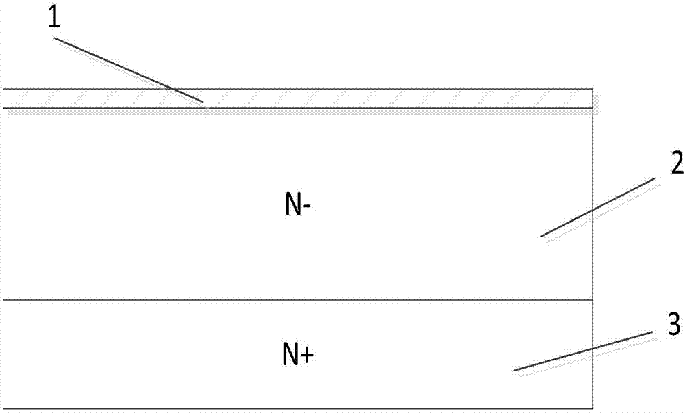
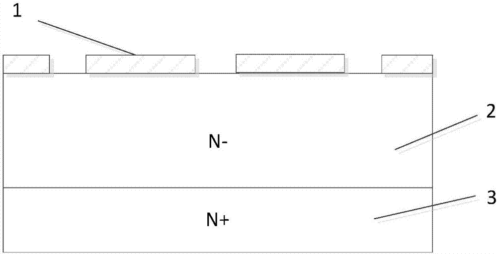
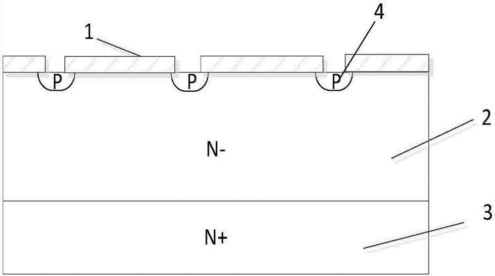
[0036] An embodiment of the present invention provides a method for manufacturing a semiconductor element, the method comprising:

[0037] Perform ion implantation at multiple preset implantation positions of the semiconductor material;

[0038] Forming a doped P-type region at each implantation position through the implanted ions, and a doped P-type diffusion region diffused from the doped P-type region;

[0039] Groove etching is performed at each implant position, and during the etching process, the doped P-type region is etched away, and the doped P-type diffusion region is retained, so that each cell of the formed semiconductor element The region has a doped P-type diffusion region.

[0040] In the embodiment of the present invention, ion implantation is performed at a plurality of preset implantation positions of the semiconductor material; through the implanted ions, a doped P-type region is formed at each implantation position, and the doped P-type region diffused in ...

Embodiment 2

[0072] Such as Figure 6 As shown, the embodiment of the present invention provides a semiconductor element, the semiconductor element is a trench structure; each trench of the trench structure corresponds to a cell region; the cell region has a doped P-type diffusion region 41 .

[0073] In the embodiments of the present invention, a doped P-type diffusion region is formed in each cell region of the semiconductor element, thereby neither reducing the device switching frequency nor the turn-on voltage drop, while effectively improving the anti-surge capability of the semiconductor element.


PUM


Abstract

The invention discloses a semiconductor component and a manufacturing method. The invention aims to improve the surge resisting capability of a high-voltage Schottky diode without reducing the switching frequency and conduction voltage drop of the device. The method comprises the following steps that: ion implantation is performed at a plurality of preset implantation positions of a semiconductor material; by means of implanted ions, doped P type regions and doped P type diffusion region diffused from the doped P type regions can be formed at each of the implantation positions; and trench etching is performed at each implantation position, and during the etching process, the doped P type regions are removed through etching, and the doped P type diffusion regions are reserved, and therefore, each cell region of a formed semiconductor component has one doped P type diffusion region.

Description

technical field [0001] The invention relates to the field of electronic devices, in particular to a semiconductor element with high surge capability and a manufacturing method. Background technique [0002] Schottky diode is a unipolar carrier device with electrons as carriers. It is widely used in switching power supplies and other high-speed power switching devices because of its low conduction voltage drop and fast switching frequency. . [0003] The most widely used in the market is TMBS (trench gate Schottky diode). In the field of high-voltage applications, since the Schottky diode is a unipolar carrier device, the bulk silicon resistivity of the device is very large, and the conduction voltage drop of the device is large, especially under the condition of large current surge, the device is easy to be damaged due to power Excessive consumption and burnt. Compared with fast recovery diodes, Schottky diodes have lower surge resistance. Contents of the invention [...

Claims


Application Information

Patent Timeline
Patent Type & Authority Applications(China)
IPC IPC(8): H01L21/329H01L29/06H01L29/872
CPCH01L29/66143H01L29/0634H01L29/8725
Inventor 单亚东谢刚张伟胡丹
Owner 广微集成技术(深圳)有限公司
Why Eureka
Try Eureka