

Semiconductor device including an insulated gate bipolar transistor and a circuit configured to control the insulated gate bipolar transistor provided on the same semiconductor substrate
a technology of insulated gate bipolar transistor and semiconductor substrate, which is applied in the direction of semiconductor devices, diodes, electrical devices, etc., can solve the problems of difficult to reduce the size or cost of chips, further reducing the size of circuit portions, and reducing the area of self-separation regions, so as to improve surge resistance and reduce the size of invalid regions , the effect of reducing the size of chips
- Summary
- Abstract
- Description
- Claims
- Application Information
AI Technical Summary
Benefits of technology
Problems solved by technology
Method used
Image

Examples
embodiment 1
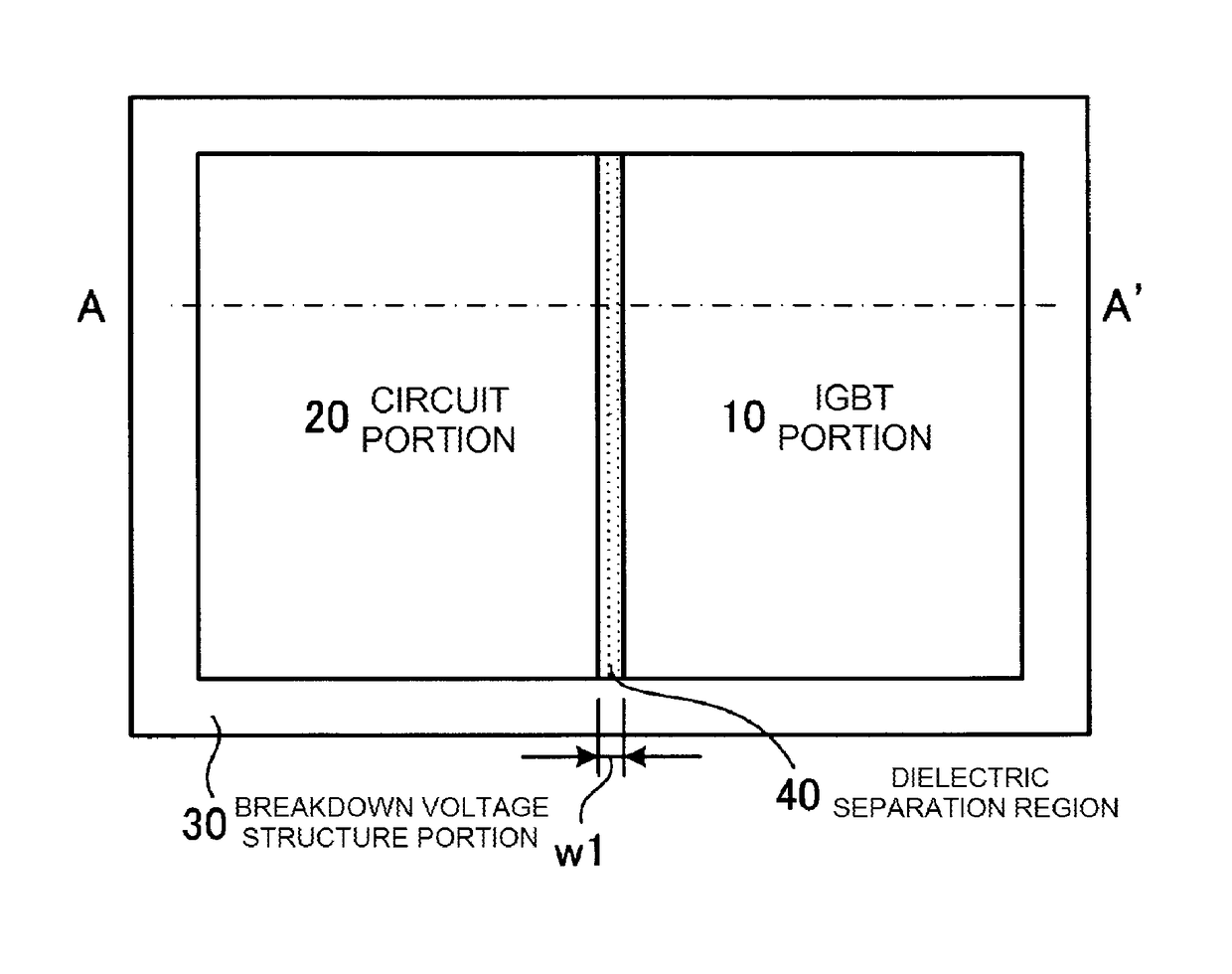
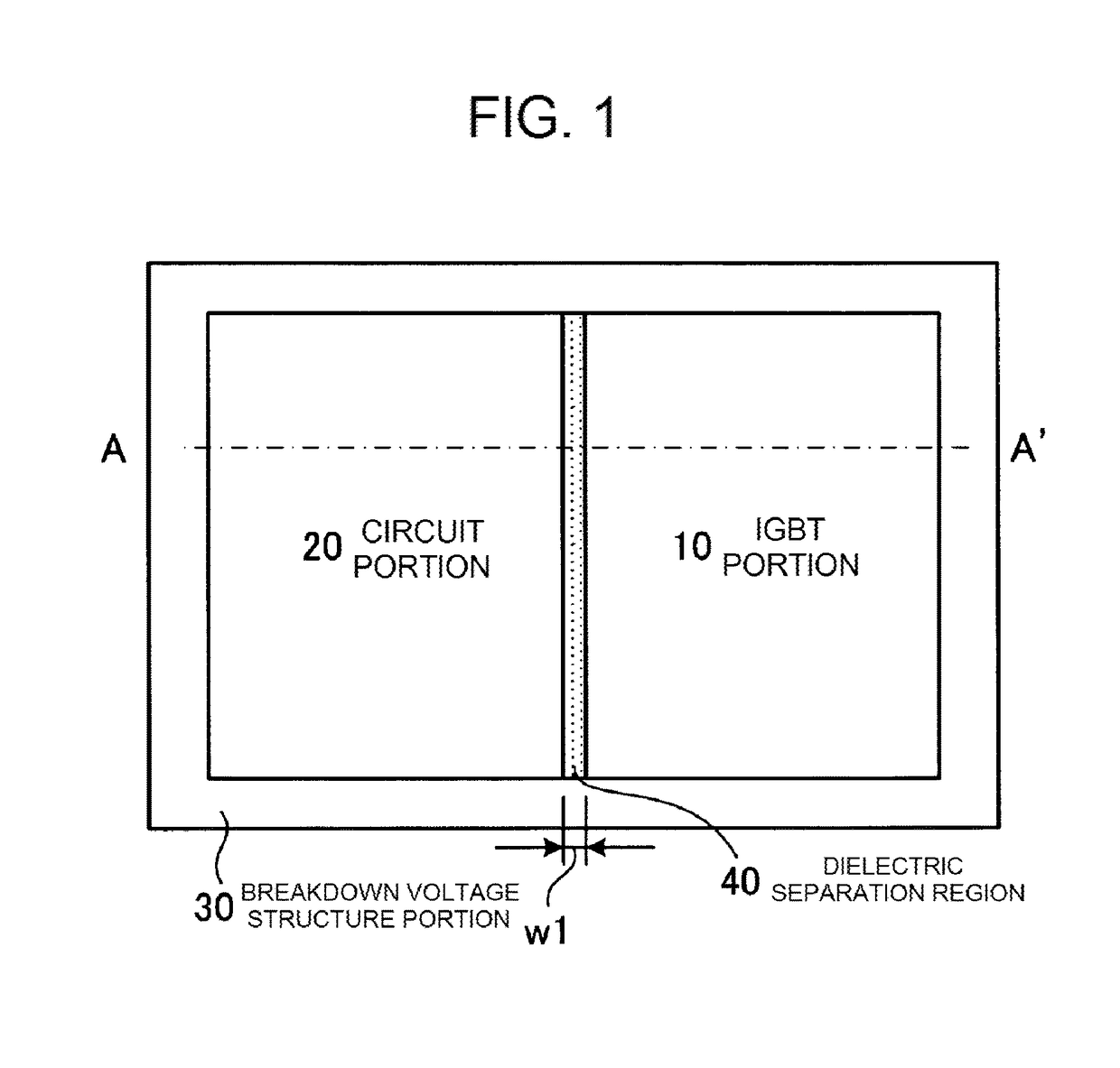
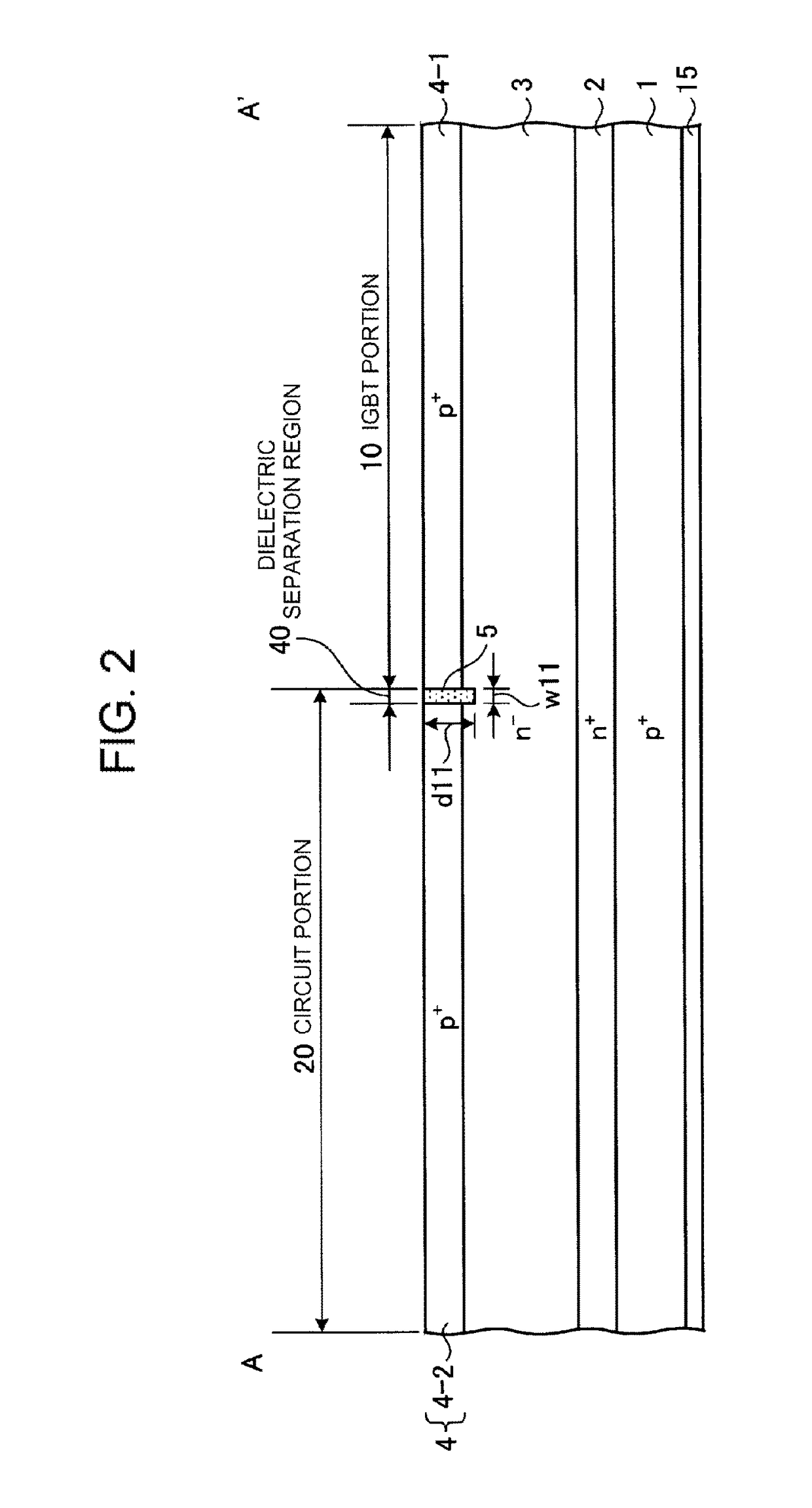
[0052]A semiconductor device in which an IGBT and a circuit portion for controlling the IGBT are provided on the same chip will be described as an example of the structure of a semiconductor device according to Embodiment 1. FIG. 1 is a plan view illustrating the planar layout of the semiconductor device according to Embodiment 1. FIG. 2 is a cross-sectional view schematically illustrating a cross-sectional structure taken along the cutting line A-A′ of FIG. 1. FIG. 3-1 is a cross-sectional view illustrating in detail the cross-sectional structure taken along the cutting line A-A′ of FIG. 1. In FIG. 2, an element structure which is formed on the front surface side of the chip is not illustrated. As illustrated in FIG. 1, in the semiconductor device according to Embodiment 1, an IGBT portion (first element portion) 10 in which the IGBT is arranged and a circuit portion (second element portion) 20 in which a plurality of elements forming a circuit for controlling the IGBT in the IGBT ...
embodiment 2
[0086]Next, a semiconductor device according to Embodiment 2 will be described. FIG. 5-1 is a cross-sectional view illustrating the structure of the semiconductor device according to Embodiment 2. FIG. 5-2 is a plan view illustrating the planar layout of an individual circuit provided in the circuit portion illustrated in FIG. 5-1 and the periphery thereof. FIG. 5-3 is a plan view illustrating the planar layout of a sense IGBT provided in the circuit portion illustrated in FIG. 5-1 and the periphery thereof. FIG. 6 is a cross-sectional view illustrating the structure of another example of the semiconductor device according to Embodiment 2. The planar layout of the semiconductor device according to Embodiment 2 is the same as that illustrated in FIG. 1. The semiconductor device according to Embodiment 2 differs from the semiconductor device according to Embodiment 1 in that an emitter contact electrode with an emitter potential (ground potential) is selectively provided in a circuit ...
embodiment 3
[0091]Next, a semiconductor device according to Embodiment 3 will be described. FIG. 7 is a plan view illustrating the planar layout of the semiconductor device according to Embodiment 3. FIG. 8-1 is a cross-sectional view schematically illustrating a cross-sectional structure taken along the cutting line B-B′ of FIG. 7. FIG. 8-2 is a cross-sectional view schematically illustrating a cross-sectional structure taken along the cutting line C-C′ of FIG. 7. FIG. 8-3 is a cross-sectional view schematically illustrating a cross-sectional structure taken along the cutting line D-D′ of FIG. 7. The arrangement of an IGBT portion 10, a circuit portion 20, a breakdown voltage structure portion 30, and a dielectric separation region 40 in FIG. 7 is the same as that in FIG. 1. The semiconductor device according to Embodiment 3 differs from the semiconductor device according to Embodiment 1 in that an emitter ring 50 is provided in the vicinity of the boundary between the IGBT portion 10 and the ...
PUM
 Abstract
Description
Claims
Application Information