Integrated circuit and manufacturing method thereof

A technology of integrated circuits and manufacturing methods, which is applied in the direction of circuits, semiconductor/solid-state device manufacturing, electrical components, etc., and can solve problems such as the inability to effectively control the size of components in the peripheral area

Pending Publication Date: 2020-10-27
WINBOND ELECTRONICS CORP
View PDF5 Cites 0 Cited by
  • Summary
  • Abstract
  • Description
  • Claims
  • Application Information

AI Technical Summary

Problems solved by technology

[0003] However, taking flash memory (flash) as an example, because most of the flash memory technology is a high-temperature process, and components with smaller dimensions (such as logic components) usually need to use a low-temperature process, if the logic components are to ...

Method used


Image

  • Integrated circuit and manufacturing method thereof
  • Integrated circuit and manufacturing method thereof
  • Integrated circuit and manufacturing method thereof

Examples


Embodiment Construction

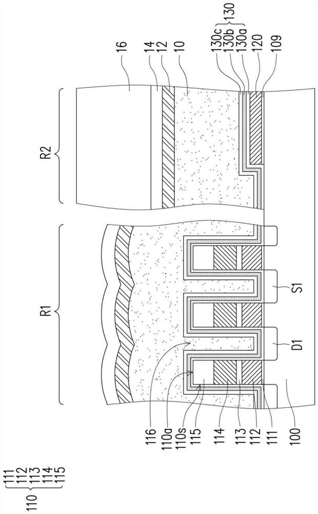
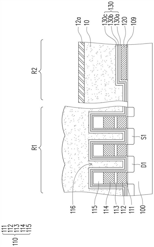
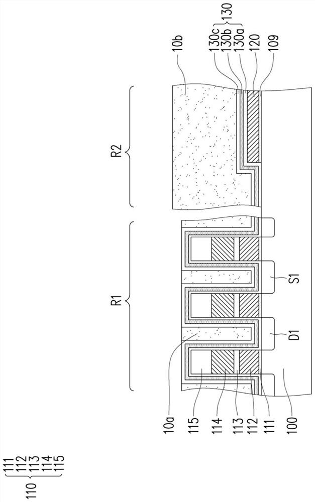
[0046] The present invention will be described more fully with reference to the accompanying drawings of this embodiment. However, the present invention can also be embodied in various forms and should not be limited to the embodiments described herein. In the drawings, the thicknesses of layers and regions may be exaggerated for clarity. The same or similar symbols represent the same or similar components, and the following paragraphs will not repeat them one by one.

[0047] Please refer to Figure 1A , this embodiment provides a method for manufacturing an integrated circuit, the steps of which are as follows. First, a substrate 100 is provided, and the substrate 100 is, for example, a silicon substrate. The substrate 100 has a cell region R1 and a peripheral region R2.

[0048] Next, a first process is performed on the substrate 100 . The first process is, for example, a flash memory process, but the invention is not limited thereto. The first process may include the...


PUM


Abstract

The invention provides an integrated circuit, which includes a substrate, a plurality of first gate structures, a compliant protection layer, a second gate structure, a source electrode region, and adrain electrode region, wherein the substrate has a cell region and a peripheral region, the plurality of first gate structures are disposed in the cell region, the compliant protective layer covers the top surface and the side wall of each first gate structure, the second gate structure is disposed in the peripheral region, and the source electrode region and the drain electrode region are disposed in the substrate on both sides of the second gate structure. The invention further provides a manufacturing method of the integrated circuit. According to the invention, the first gate structure can be protected from interference of moving ions, and damage of the moving ions to the component is avoided; and the diffusion of the source electrode region and the drain electrode region can be effectively controlled, and the assembly of the peripheral region is controlled at a relatively small gate length, so that the assembly size of the peripheral region in the integrated circuit can be reduced.

Description

technical field [0001] The invention relates to an integrated circuit and a manufacturing method thereof, in particular to an integrated circuit capable of effectively reducing the size and a manufacturing method thereof. Background technique [0002] With the rapid development of science and technology, in order to meet the needs of reducing costs and simplifying process steps, semiconductor components integrate smaller components (such as logic components) into the peripheral region of the integrated circuit, thereby reducing the size of the peripheral region of the integrated circuit. Gradually become a trend. [0003] However, taking flash memory (flash) as an example, because most of the flash memory technology is a high-temperature process, and components with smaller dimensions (such as logic components) usually need to use a low-temperature process, if the logic components are to be integrated into the flash memory If there is a peripheral region, the source region ...

Claims


Application Information

Patent Timeline
IPC IPC(8): H01L27/11524H01L27/11529H01L27/11536H01L21/768
CPCH01L21/76847H10B41/35H10B41/44H10B41/41
Inventor 蔡耀庭庄哲辅张荣和廖修汉
Owner WINBOND ELECTRONICS CORP
Why Eureka
Try Eureka