Organic electroluminescence display device
An electroluminescence display and display device technology, which is applied in the direction of electroluminescence light sources, electric light sources, lighting devices, etc., can solve problems such as manufacturing difficulties and insufficient selectivity
- Summary
- Abstract
- Description
- Claims
- Application Information
AI Technical Summary
Problems solved by technology
Method used
Image

Examples
no. 1 approach
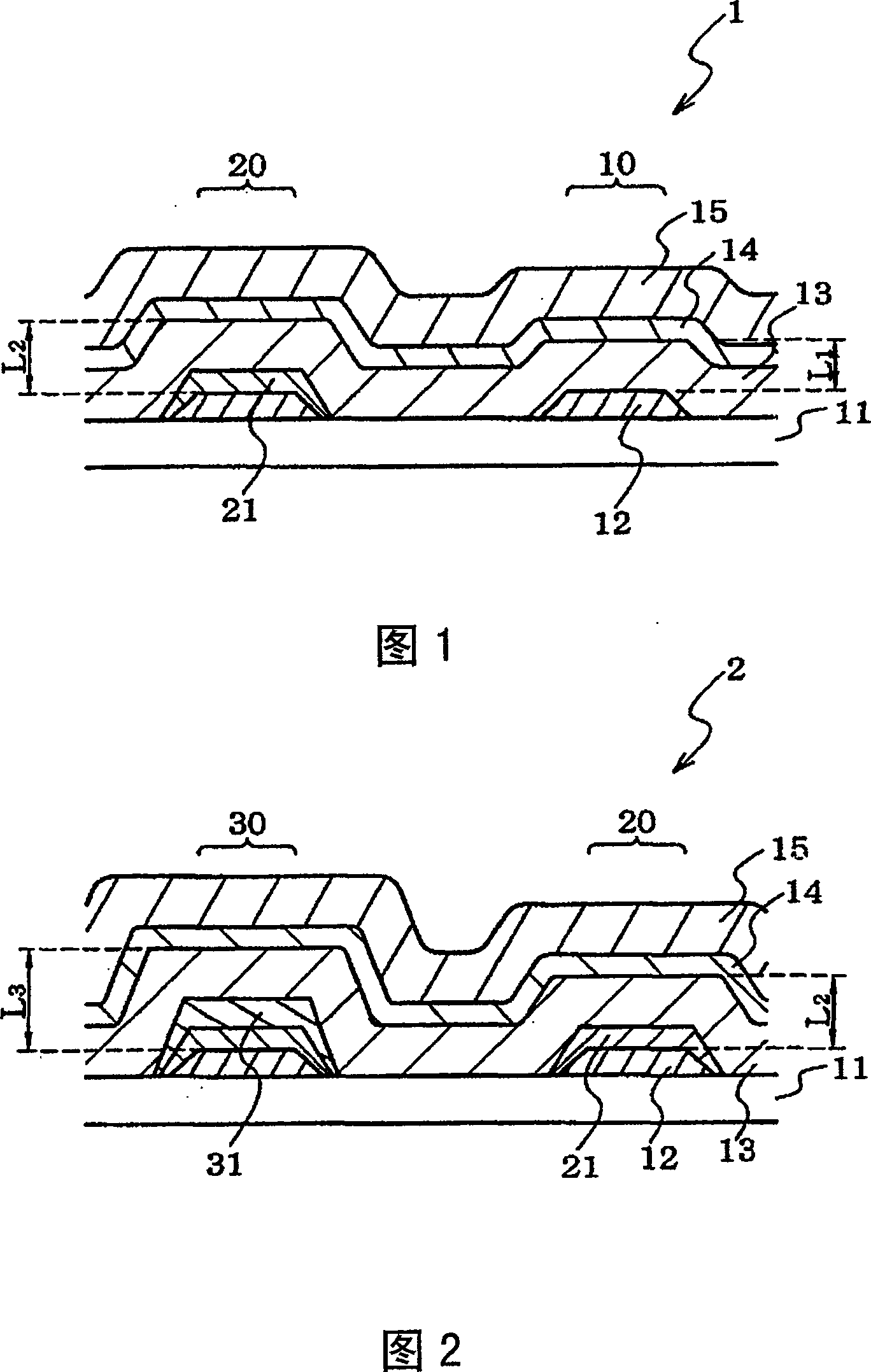
[0047] FIG. 1 is a diagram showing an organic EL display device according to a first embodiment of the present invention.
[0048] The organic EL display device 1 has a first organic EL element portion 10 and a second organic EL element portion 20 juxtaposed on a substrate 11 .
[0049] The first organic EL element unit 10 has a structure in which a light-reflective conductive layer 12 , an organic light-emitting medium layer 13 , a light-reflective layer 14 , and a transparent electrode layer 15 are sequentially stacked on a substrate 11 .
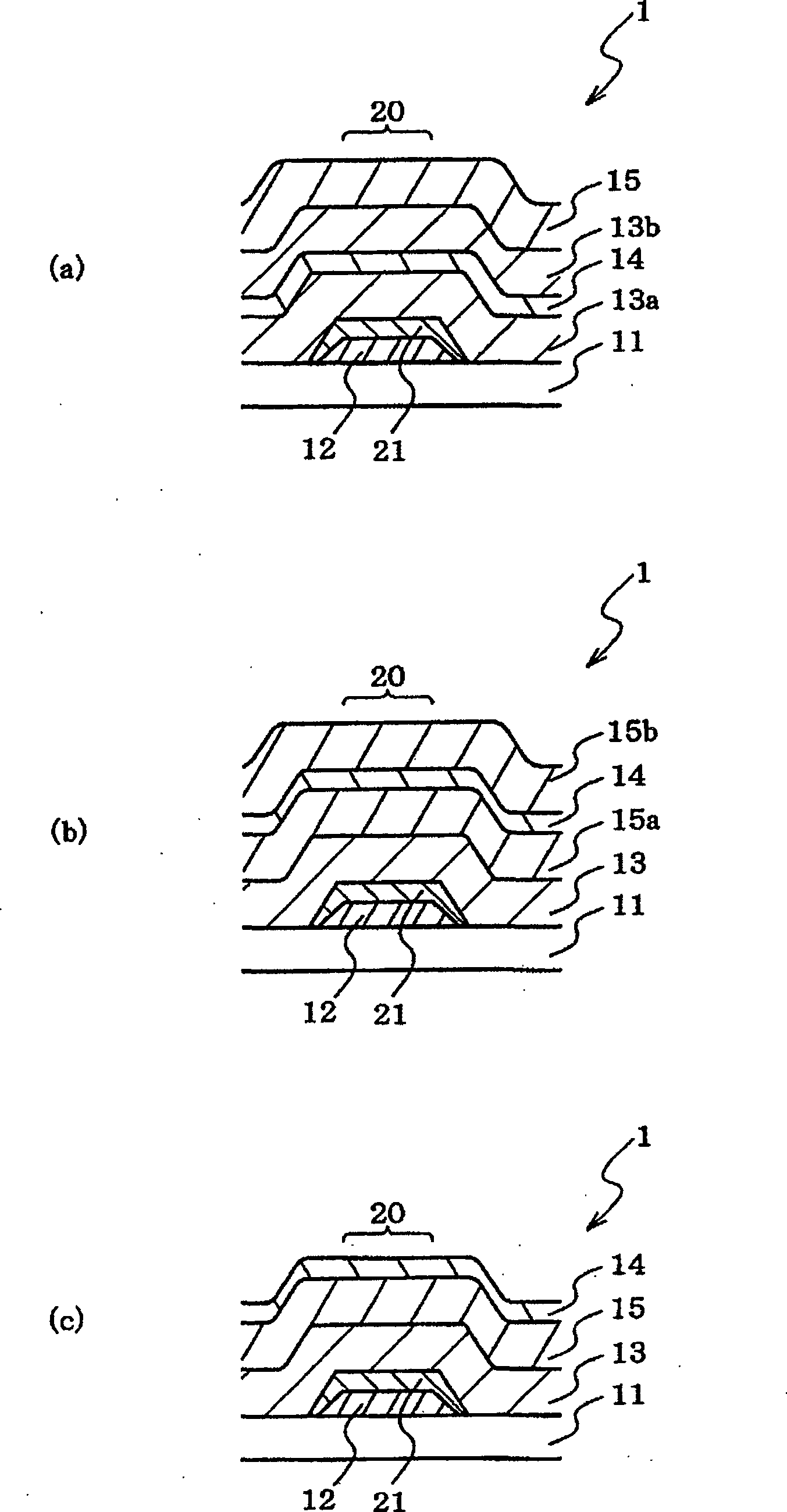
[0050] The second organic EL element unit 20 has a structure in which a light reflective conductive layer 12 , a first inorganic compound layer 21 , an organic luminescent medium layer 13 , a light reflective layer 14 , and a transparent electrode layer 15 are sequentially stacked on a substrate 11 .
[0051] The light-reflecting conductive layer 12 is a layer that functions as an electrode for supplying holes or electrons and reflects li...
no. 2 approach
[0061] FIG. 2 is a diagram showing an organic EL display device according to a second embodiment of the present invention.
[0062] The organic EL display device 2 has a second organic EL element unit 20 and a third organic EL element unit 30 provided side by side on a substrate 11 .
[0063] The second organic EL element portion 20 is the same as that of the first embodiment described above.
[0064] The third organic EL element part 30 has a light-reflective conductive layer 12, a first inorganic compound layer 21, a second inorganic compound layer 31, an organic light-emitting medium layer 13, a light-reflective layer 14, and a transparent electrode layer 15 stacked in this order on the substrate 11. Structure. That is, the function of each layer is the same as that of the second organic EL element portion 20 except for the formation of the second inorganic compound layer 31 .
[0065] The second inorganic compound layer 31 formed on the third organic EL element portion 3...
no. 3 approach
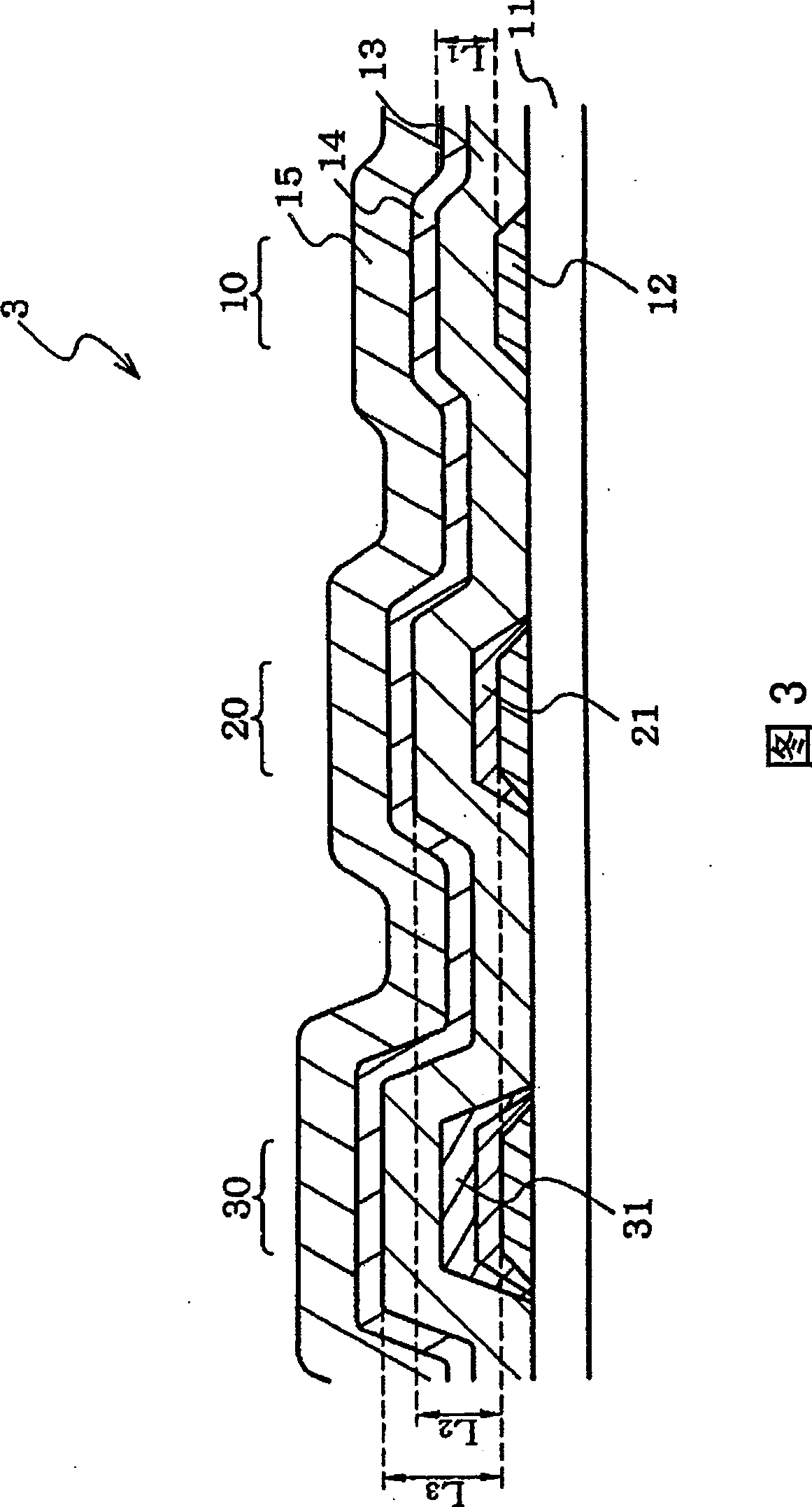
[0071] FIG. 3 is a diagram showing an organic EL display device according to a third embodiment of the present invention.
[0072] The organic EL display device 3 has a first organic EL element portion 10 , a second organic EL element portion 20 , and a third organic EL element portion 30 juxtaposed on a substrate 11 .
[0073] The structure of each organic EL element part 10, 20, 30 is the same as that of the said 1st and 2nd embodiment, and the function of each layer is also the same.
[0074] In the organic EL display device 3 , the organic EL element portions 10 , 20 , and 30 each have a resonator structure having a different optical distance (optical film thickness). That is, the optical distance is L1 in the first organic EL element section 10 , L2 in the second organic EL element section 20 , and L3 in the third organic EL element section 30 .
[0075] Therefore, in each of the organic EL element portions 10 , 20 , and 30 , lights (λ1, λ2, and λ3) having different wave...
PUM
 Abstract
Description
Claims
Application Information
 - R&D
- Intellectual Property
- Life Sciences
- Materials
- Tech Scout
- Unparalleled Data Quality
- Higher Quality Content
- 60% Fewer Hallucinations
Browse by: Latest US Patents, China's latest patents, Technical Efficacy Thesaurus, Application Domain, Technology Topic, Popular Technical Reports.
© 2025 PatSnap. All rights reserved.Legal|Privacy policy|Modern Slavery Act Transparency Statement|Sitemap|About US| Contact US: help@patsnap.com