Image display apparatus and high voltage driver circuit

A technology of image display device and driver circuit, which is applied in image communication, static indicator, color signal processing circuit, etc., can solve the problems of limiting the speed of push-pull level, which is not conducive to driving display screen devices, etc.

Inactive Publication Date: 2009-09-16
ENTROPIC COMM INC
View PDF6 Cites 0 Cited by
  • Summary
  • Abstract
  • Description
  • Claims
  • Application Information

AI Technical Summary

Problems solved by technology

However, unless large input currents of both positive and negative polarities are available, the amplifier must rely on current mirror amplification to amplify
Therefore an amplified P-type current mirror must be u

Method used


Image

  • Image display apparatus and high voltage driver circuit
  • Image display apparatus and high voltage driver circuit

Examples


Embodiment Construction

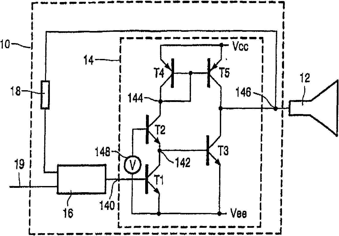
[0026] figure 1 An image display device is shown having a driver circuit 10 comprising a driver stage 14 , a preamplifier 16 and a feedback circuit 18 and a display screen assembly 12 of a CRT. The input 19 of the driver circuit 10 is connected to an input of a preamplifier 16 having an output connected to the input of the driver stage 14 . The output of the driver stage 14 is connected to a control electrode of the image display device 12 and to a further input 19 of a preamplifier 16 via a feedback circuit 18 . The driver stage 14 comprises an input transistor T1 of NPN type, a control transistor T2 of NPN type, a pull transistor T3 of NPN type and a current mirror T4, T5 having a mirror input transistor T4 of PNP type and a mirror output transistor of PNP type T5, the input 140 of the driver stage 14 is connected to the control electrode of the input transistor T1. The main current channel of the input transistor T1 is connected between the first power supply Vee and the ...


PUM


Abstract

A driver circuit for an image display device includes a driver circuit with A/B class push-pull stages (T3, T5). The driver circuit consists of an N-type pull transistor (T3), an N-type control transistor (T2), the main current channel terminal of T2 is connected to the control electrode of the pull transistor (T2), and a voltage source (V) is used to control A predetermined voltage is applied across the series connection of the control electrode main current path terminal of the transistor (T2) and the pull transistor (T3). The current from the control transistor (T2) flows to the p-type push transistor (T5) via the current mirror (T4, T5). The input transistor (T1) draws all the current from the control transistor (T2) via the node (142) between the control transistor (T2) and the pull transistor (T3) to control the current flow through these transistors (T2, T3). ratio between. The input to the driver circuit has direct control of the current through the input transistor (T1), which does not include feedback through the control transistor (T2).

Description

technical field [0001] The present invention relates to an image display device, a high voltage driver circuit for driving a display screen in such a device, and more generally to a high voltage driver circuit. Background technique [0002] A high voltage swinging at a high frequency is required to drive an image display screen device such as a CRT. The swing of the output can be greater than 100 volts, which makes minimizing the amount of current that causes power dissipation in the driver circuit in the display screen device a task of first importance. Well known techniques for minimizing power dissipation in the driver circuit are , using a class A / B push-pull output stage. A class A / B push-pull output stage is an output stage that sinks some quiescent current but can source more output current than the quiescent current. [0003] The class A / B output stage includes a pull-up transistor connected between the output and the first power supply, and a pull-up transistor co...

Claims


Application Information

Patent Timeline
IPC IPC(8): H03F3/30H04N9/64G09G1/00H04N5/14
CPCH04N5/148H03F3/3067G09G1/00
Inventor M·H·斯里托夫
Owner ENTROPIC COMM INC
Why Eureka
Try Eureka