

Luminous device, method of manufacturing luminous device and electronic device
A light-emitting device and manufacturing method technology, applied in the direction of electroluminescent light source, identification device, lighting device, etc., can solve the problem of not being able to contribute to the display, etc.
- Summary
- Abstract
- Description
- Claims
- Application Information
AI Technical Summary
Problems solved by technology
Method used
Image

Examples
no. 1 approach
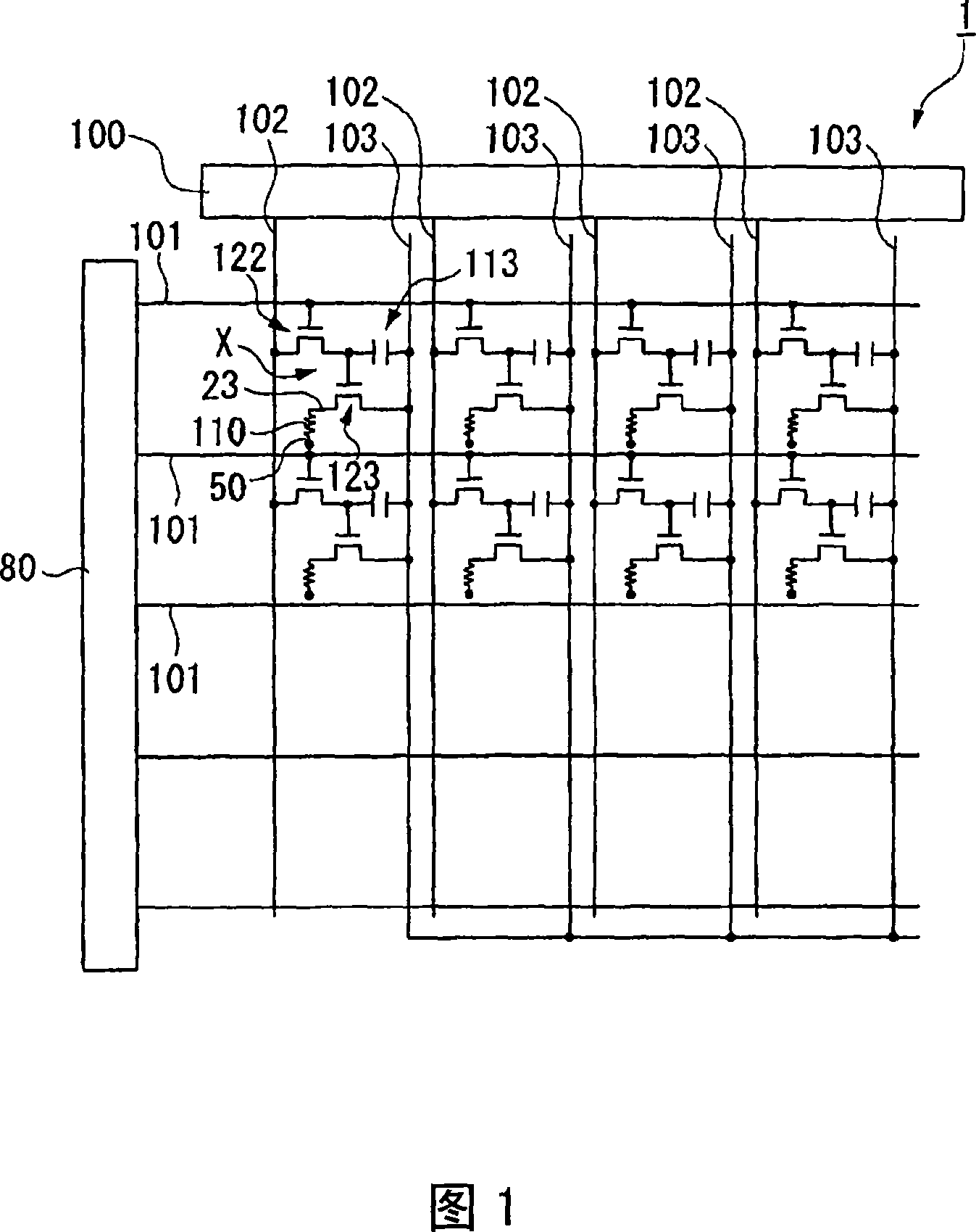
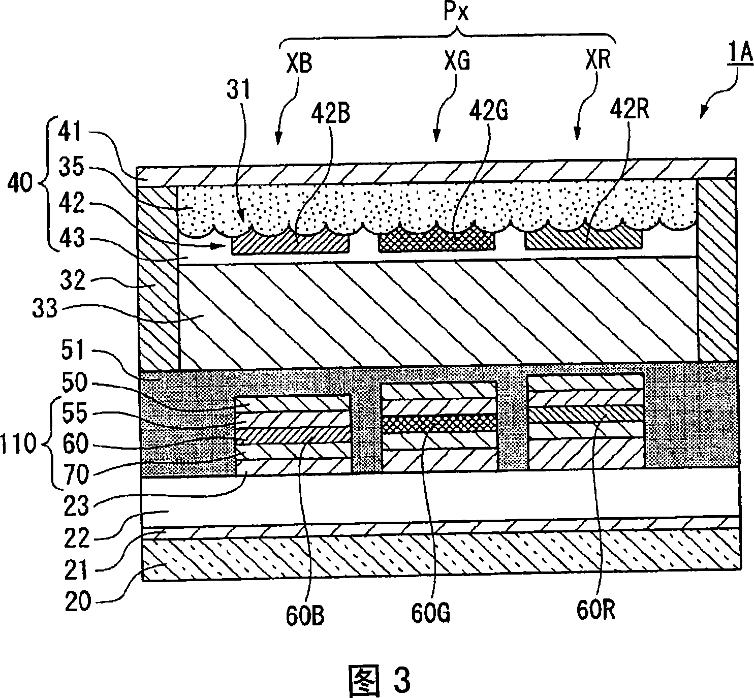
[0082] Next, referring to FIG. 3 , in the first embodiment of the organic EL elements constituting the organic EL panel 1 , the structure of the unit pixel group of the organic EL elements will be described.
[0083] In addition, in FIG. 3 , the pixel electrode 23 , the light-emitting functional layer 110 , and the cathode 50 constituting the organic EL element are described in detail, and the driving TFT 123 is connected to the pixel electrode 23 . In addition, the pixel electrodes 23 are respectively formed on the red pixel XR, the green pixel XG, and the blue pixel XG, and as shown in FIG. 1 , each pixel is made to emit light by the action of the driving TFT 123 .
[0084] As shown in FIG. 3 , the unit pixel group Px of the organic EL element (organic EL device) 1A includes a light-emitting functional layer 110 sandwiched between the pixel electrode 23 and the cathode 50 on the substrate 20 . In addition, a color filter substrate 40 is provided to face the substrate 20 , an...
no. 4 approach
[0123] Next, the structure of the unit pixel group of the organic EL element constituting the fourth embodiment of the organic EL element of the organic EL panel 1 will be described with reference to FIG. 15 .
[0124] In addition, FIG. 15 is a diagram corresponding to FIG. 3 showing the first embodiment of the organic EL element, and the same symbols as those shown in FIG. Component composition.
[0125] In the organic EL element 1D of the fourth embodiment, the structure of the color filter substrate 40 is different from that of the organic EL element 1A of the first embodiment. Specifically, the color filter substrate 40 includes a substrate 41 made of a light-transmitting member such as a glass material, and a color filter layer 42 ( 42B, 42G, 42R) formed on the substrate 41 to cover the color filter layer 42 . In addition to the cover layer 43 formed in this manner, the substrate 41 is further provided with a directional scattering layer 35 on the side different from the...
no. 6 approach
[0142] Next, the structure of the unit pixel group of the organic EL element constituting the sixth embodiment of the organic EL element of the organic EL panel 1 will be described with reference to FIG. 20 .
[0143] In addition, FIG. 20 is a diagram corresponding to FIG. 3 showing the first embodiment of the organic EL element, and the same symbols as those shown in FIG. Component composition.
[0144] The organic EL element 1F of the sixth embodiment is a bottom emission type organic EL element in which light emitted from the light-emitting functional layer 110 is emitted from the side of the substrate 20 including the pixel electrode 23 .
[0145] The organic EL element 1F includes a protective layer 22 on a substrate 20 made of a light-transmitting material such as glass, and includes a directional scattering layer 35 on the protective layer 22 . Furthermore, a laminated body composed of the pixel electrode 23 , the light-emitting functional layer 110 , the cathode 50 , ...
PUM
 Abstract
Description
Claims
Application Information