Method for raising fine quality of semiconductor chip
A yield, semiconductor technology, used in semiconductor/solid-state device manufacturing, photoengraving process of patterned surface, optics, etc., can solve the problems of yield reduction, negative photoresist residue, etc., and achieve the effect of improving yield
- Summary
- Abstract
- Description
- Claims
- Application Information
AI Technical Summary
Problems solved by technology
Method used
Image

Examples
Embodiment Construction
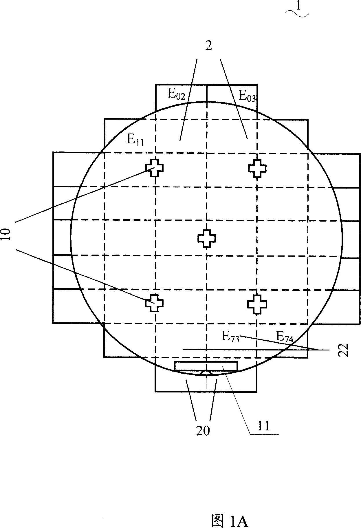
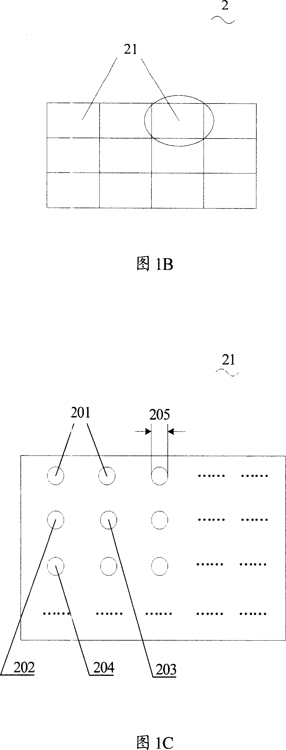
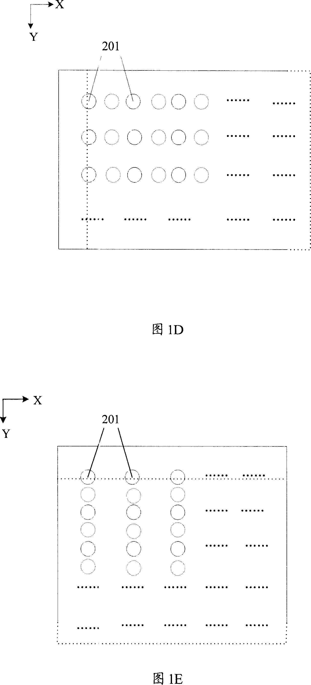
[0030] Due to the use of double exposure in the wafer identification code area, the exposure energy is enhanced, which exposes the edges of several chips in the non-wafer identification code area connected to the wafer identification code area, forming negative photoresist residues, which makes the original soldering The area of the bump disappears, resulting in a decrease in yield. In order to improve the above situation, the present invention adopts the following method to perform double exposure on the wafer identification code area.
[0031] Please refer to shown in Fig. 3, the method for improving the yield rate of semiconductor chips of the present invention includes the following steps: coating a layer of negative photoresist S101 on the wafer surface; aligning the wafer identification code area with the photomask S102; Based on the exposure energy of the non-wafer identification code area, perform the first exposure S103 in the wafer identification code area; offset ...
PUM
| Property | Measurement | Unit |
|---|---|---|
| thickness | aaaaa | aaaaa |
Abstract
Description
Claims
Application Information