Semiconductor chip packaging structure

A chip packaging structure, semiconductor technology, applied in the direction of semiconductor devices, semiconductor/solid-state device components, electric solid-state devices, etc., can solve the problems of the limited number of semiconductor chip packages, difficulty in meeting light concentration requirements, and inability to concentrate semiconductor chips

Inactive Publication Date: 2008-03-12
LEADER ELECTRONICS
View PDF1 Cites 0 Cited by
  • Summary
  • Abstract
  • Description
  • Claims
  • Application Information

AI Technical Summary

Problems solved by technology

Although this kind of package structure can solve the heat dissipation problem of packaging multiple high-power chips, because only one side of the package structure can be attached to the semiconductor chip, the number of packages of the semiconductor chip is limited, and when the semiconductor chip is In the case of light-emitting diodes, because the semiconductor chips distributed around the package structure cannot be concentrated, it is difficult to meet the light-gathering requirements when applied to semiconductor light source devices.

Method used


Image

  • Semiconductor chip packaging structure
  • Semiconductor chip packaging structure
  • Semiconductor chip packaging structure

Examples


Embodiment Construction

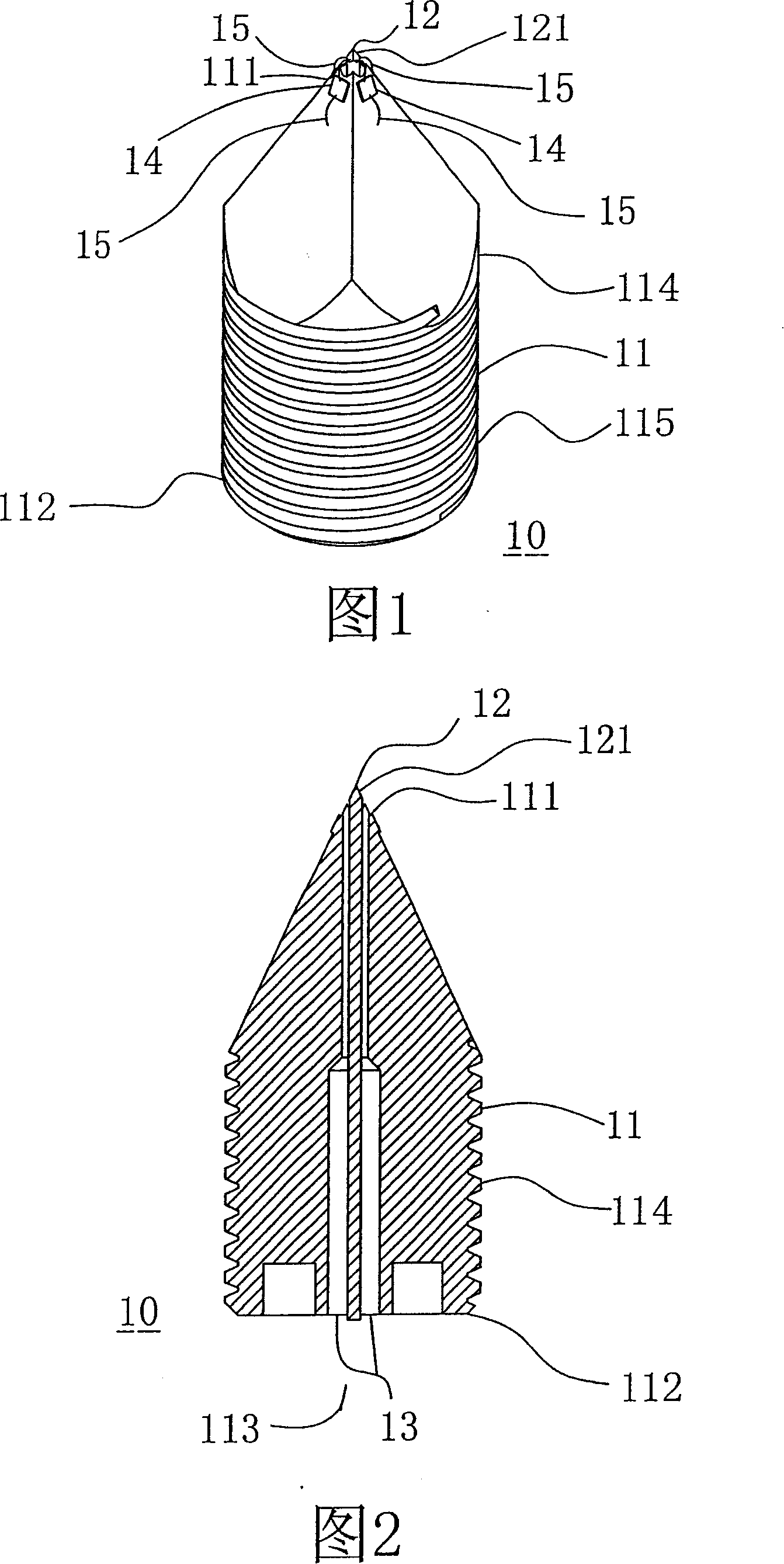
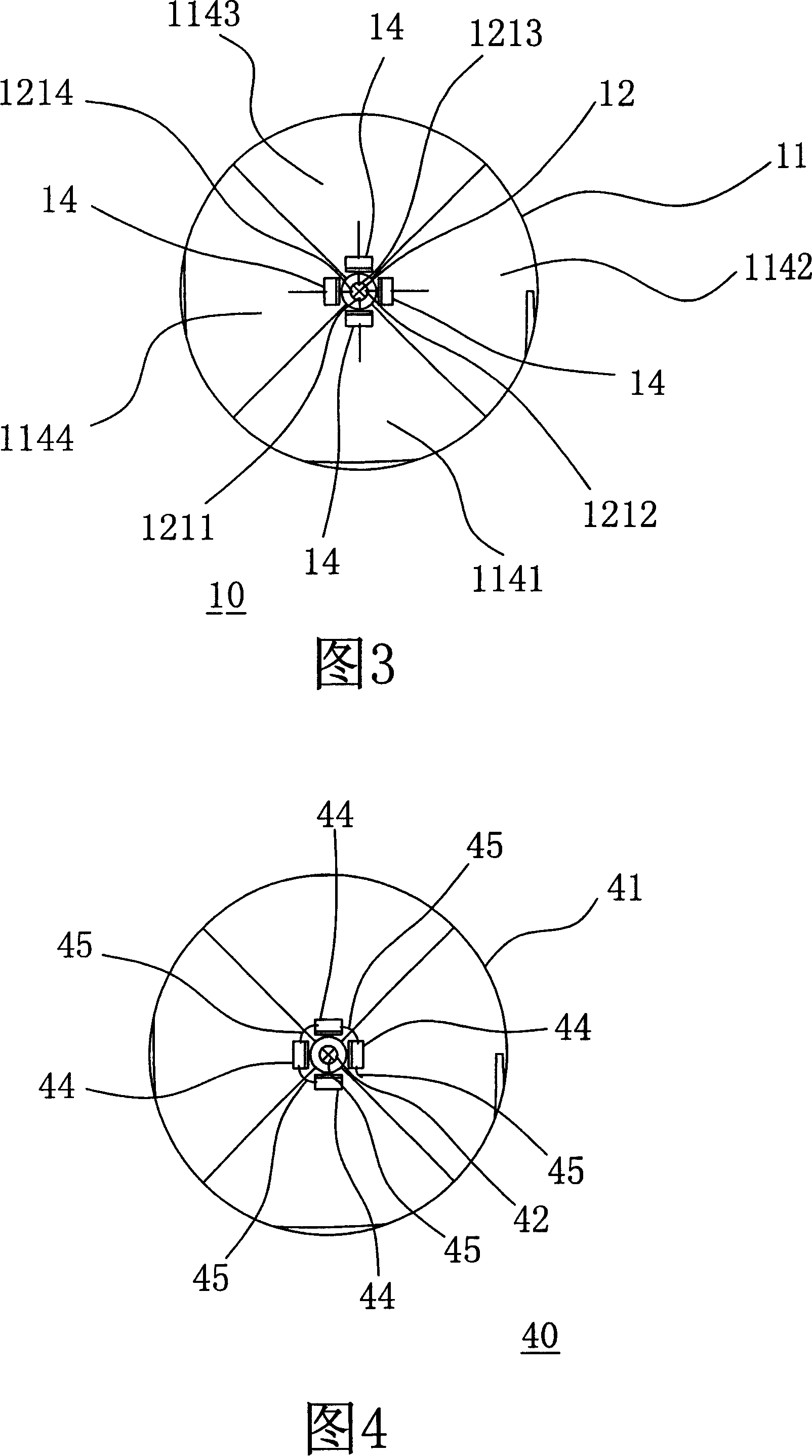
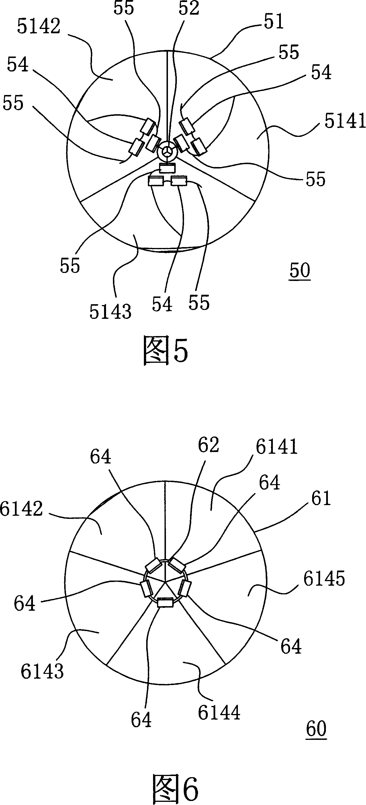
[0036] 1-3 show a semiconductor chip package structure 10 according to the first embodiment of the present invention. The semiconductor chip package structure 10 includes an outer conductor 11 , an inner conductor 12 , an insulating layer 13 and a plurality of semiconductor chips 14 .

[0037] As shown in the figure, the outer conductor 11 is preferably a long cylindrical shape, which has a first end 111 , a second end 112 , a through hole 113 connecting the first end 111 and the second end 112 , and an outer surface 114 . The first end 111 is made into a cone shape, and the cone-shaped outer surface 114 has planes 1141 , 1142 , 1143 , and 1144 evenly distributed around the outer conductor 11 for attaching semiconductor chips 14 such as LEDs. The second end 112 can be provided with a plurality of threads 115, so that when the semiconductor chip package structure 10 is applied to the semiconductor light source device 70 (as shown in FIG. At the focal point of the spotlight cup ...


PUM


Abstract

A package structure for the semiconductor chip is provided, which is to set the inner conductor in the center pylome of the outer conductor jutting from one end of the outer conductor, wherein taking the insulated barrier as the isolation, attach a plurality of semiconductor chip onto the adjoining position of the outer conductor and inner conductor which is favorable to connect the semiconductor chip onto the inner conductor and outer conductor as the current electrode in series, parallel or series-parallel connection. Besides, set the light source used in the package structure of the semiconductor chip into the shell with spot light cup to form a semiconductor light source device with functions of both light gathering and radiating.

Description

technical field [0001] The invention relates to a semiconductor chip packaging structure, and in particular to a semiconductor chip packaging structure with both light concentrating and heat dissipation and an application device thereof. Background technique [0002] The application of known semiconductor chips such as light-emitting diodes (LEDs) must be packaged in a packaging structure and lead out electrodes, so as to facilitate users to connect power supply to make them work or emit light. [0003] For a single low-power LED, heat dissipation is not the main consideration of the packaging structure. Recently, in order to increase the application range of LEDs, multi-chip, high-power LED packaging has become an inevitable trend requirement. For example, U.S. Patent No. 6,492,725 titled "Concentrically Leaded Power Semiconductor Device Package" proposes a concentric package structure to facilitate the heat dissipation of a structure packaged with multiple high-power chip...

Claims


Application Information

Patent Timeline
Patent Type & Authority Applications(China)
IPC IPC(8): H01L25/00H01L23/488
Inventor 陈国禔
Owner LEADER ELECTRONICS
Why Eureka
Try Eureka