Metal layer and insulation layer graphic alignment error electricity testing structure in micromotor system apparatus process

A micro-electromechanical system, alignment error technology, applied in micro-structure technology, micro-structure devices, piezoelectric/electrostrictive/magnetostrictive devices, etc., can solve problems such as registration error extraction, and achieve consistent measurement methods. Simple test method and simple test equipment

Inactive Publication Date: 2008-03-19
SOUTHEAST UNIV
View PDF0 Cites 1 Cited by
  • Summary
  • Abstract
  • Description
  • Claims
  • Application Information

AI Technical Summary

Problems solved by technology

At present, electrical parameters, geometric dimension parameters and errors can be extract

Method used


Image

  • Metal layer and insulation layer graphic alignment error electricity testing structure in micromotor system apparatus process
  • Metal layer and insulation layer graphic alignment error electricity testing structure in micromotor system apparatus process
  • Metal layer and insulation layer graphic alignment error electricity testing structure in micromotor system apparatus process

Examples


Embodiment Construction

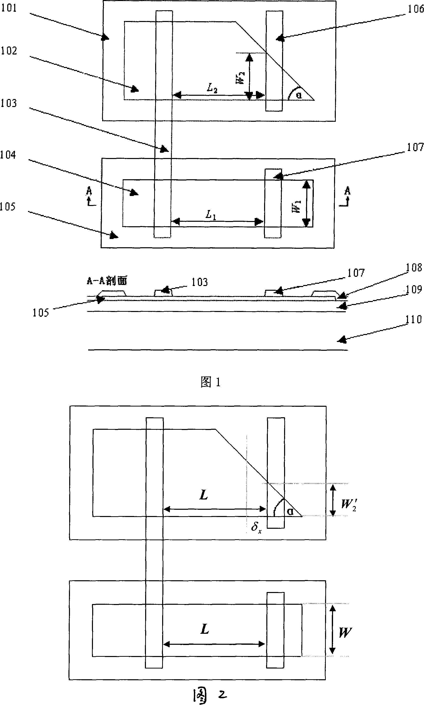
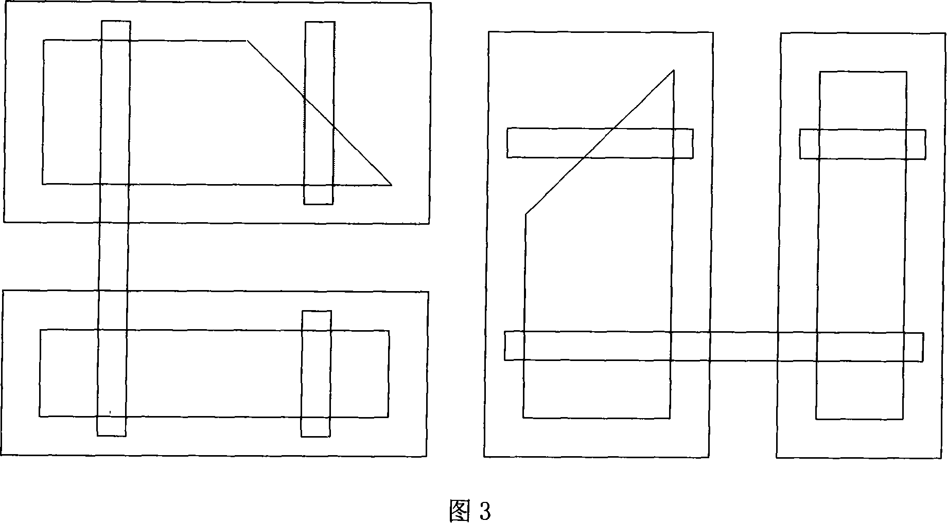
[0014] Referring to FIG. 1, a test structure pattern of the pattern error of the metal layer pattern aligned with the insulating layer pattern is given, and the cross-sectional structure of the structure is also shown in the figure. In the test structure, 101 and 105 are two rectangular semiconductor conductive materials, which provide resistance characteristics for auxiliary measurement. In the MEMS process, the material can be polysilicon, underneath them is an insulating layer material 109, usually Silicon nitride. 102 is a trapezoidal hole structure, which is a hole opened in the insulating layer 108, so that the other semiconductor conductive layer underneath is exposed, and presents a trapezoidal window pattern, and the oblique side of the trapezoid has an inclination angle α. 104 is similar to 102 in that it is also a hole, which is a rectangular window pattern on an insulating layer 108. 103, 106, and 107 are strip-shaped metal layer materials. 110 is a silicon substrate m...


PUM


Abstract

The invention relates to an electricity test structure for metal layer and insulation layer graphics alignment error in processing of micro-electro-mechanical system components. A metal layer is taken as the base layer to design an alignment error test structure; in the structure, a semiconductor layer includes two rectangular semiconductors which are separated and arranged in parallel, and made of the same material; the positions on a lower insulation layer respectively corresponding to the two semiconductors are provided with a trapezoidal and a rectangular windows, which contact with the semiconductor layer; the connected metal layer formed includes two paralleled metal bars with spacing, one of which is vertically covered on an upper and a lower bottom sides of the trapezoidal window as well as two long sides of the rectangular window, and the other is covered on the obtuse angle part of the trapezoidal window and two long sides of the rectangular window, and cut off in the separation area between the two semiconductors; the two metal bars and the semiconductors between the metal bars form a resistance with connecting wires; when relative deflection exists between the metal layer graphics and the insulation layer graphics, the testing resistance changes, and the error of the metal layer and insulation layer graphics alignment deflection can be obtained.

Description

Technical field [0001] The invention relates to a microelectromechanical system (MEMS) device processing technology, in particular to an electrical test structure for pattern alignment errors between a metal layer and an insulating layer in the processing of a microelectromechanical system device, which belongs to the field of electricity and semiconductors. Background technique [0002] There are many layers of materials in the processing of microelectromechanical systems (MEMS) devices, including both conductive layer materials and insulating layer materials. There is an overprint alignment problem between these material layer patterns, that is, there is a requirement for subsequent material layer patterns to align with the previous material layer patterns. [0003] The traditional register engraving alignment is to adopt the method of mutual nesting of large and small graphics, that is, design the same graphics of different sizes on different layers with registration requireme...

Claims


Application Information

Patent Timeline
IPC IPC(8): B81C5/00G01B7/00B81C99/00
Inventor 李伟华钱晓霞
Owner SOUTHEAST UNIV
Why Eureka
Try Eureka