Pixel structure and its manufacturing method

A technology of pixel structure and manufacturing method, which is used in semiconductor/solid-state device manufacturing, optics, instruments, etc., can solve the problems of inconsistent parasitic capacitance and uneven display, and achieve the effect of reducing parasitic capacitance and reducing parasitic capacitance.

Inactive Publication Date: 2008-04-02
AU OPTRONICS CORP
View PDF0 Cites 2 Cited by
  • Summary
  • Abstract
  • Description
  • Claims
  • Application Information

AI Technical Summary

Problems solved by technology

[0010] Therefore, the purpose of the present invention is to provide a pixel structure and its manufacturing method, in the case of reducing the parasitic capacitance as much as possible, to solve the existing method due to the inconsistency of the parasitic capacitance between the data wiring and the light-shielding metal layer on both sides resulting in uneven display

Method used


Image

  • Pixel structure and its manufacturing method
  • Pixel structure and its manufacturing method
  • Pixel structure and its manufacturing method

Examples


no. 1 example

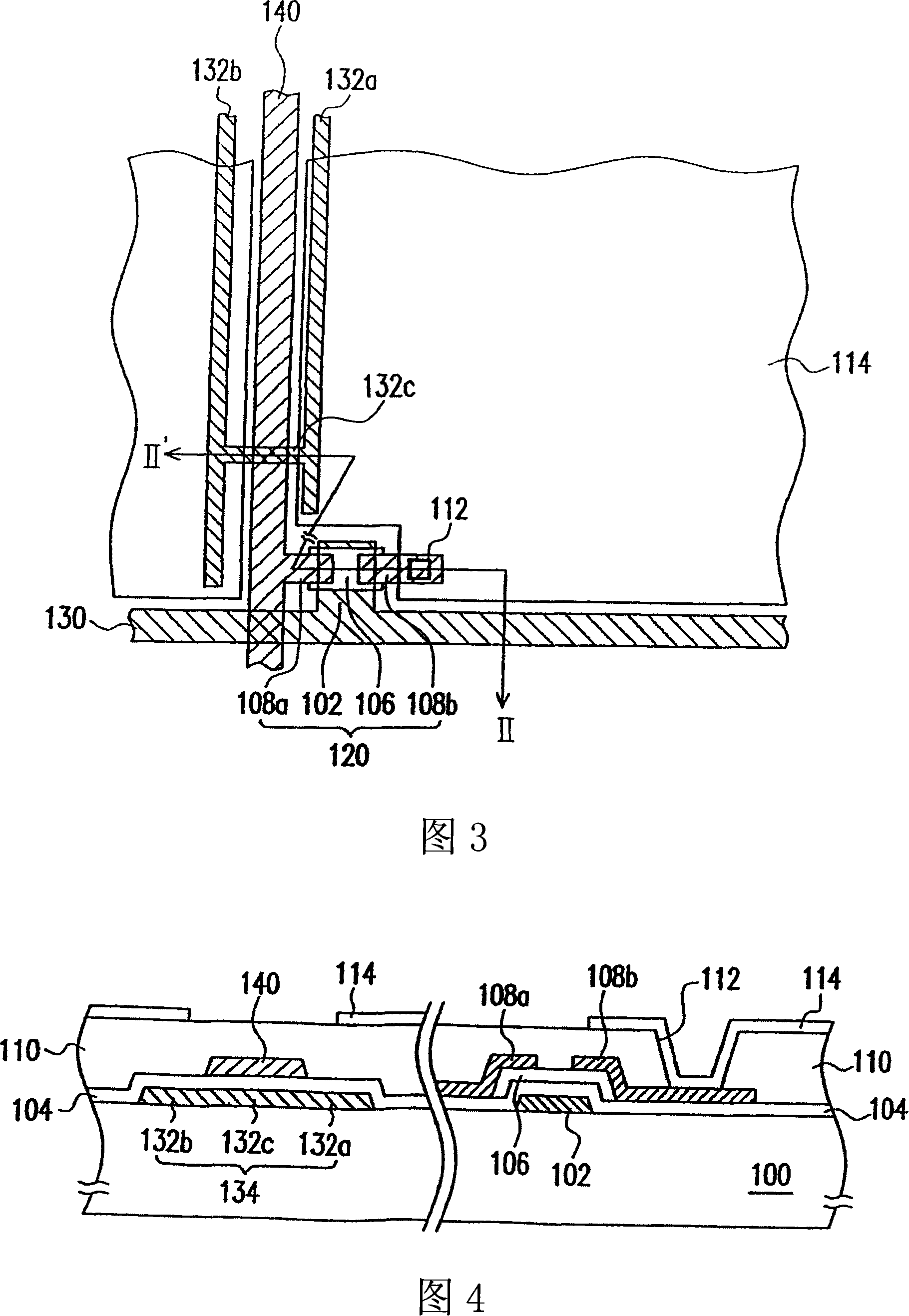
[0033] As shown in FIG. 3 , it is shown as the above-mentioned schematic diagram of a pixel structure according to a preferred embodiment of the present invention; as shown in FIG. 4 , it is shown as a schematic cross-sectional view from II-II' in FIG. 3 .

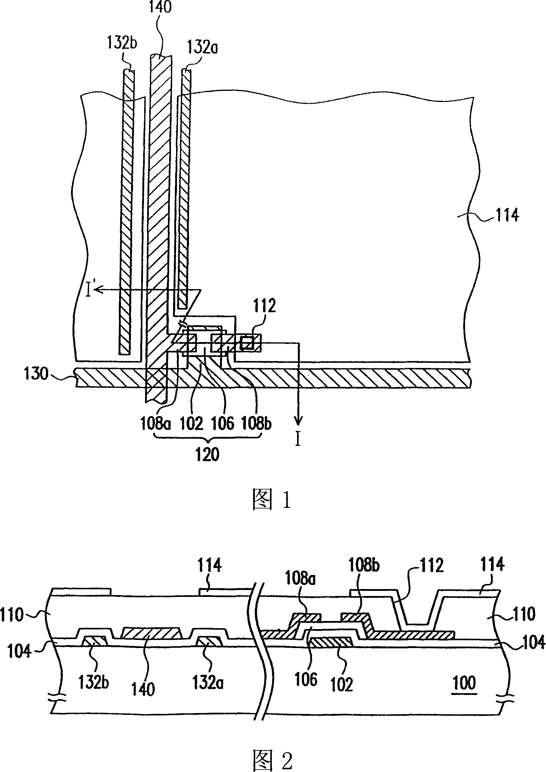
[0034] Referring to FIG. 3 and FIG. 4 , firstly, a transparent substrate 100 is provided, wherein the transparent substrate 100 is, for example, a glass substrate or a plastic substrate. Next, a gate 102 and a scan line 130 connected to the gate 102 are formed on the transparent substrate 100 , and a light-shielding layer 134 is formed on the transparent substrate 100 at the same time. Wherein, the light-shielding layer 134 is composed of a light-shielding portion 132a, 132b and a connecting portion 132c, and the light-shielding portion 132a, 132b is arranged on both sides of a predetermined data wiring, and the connecting portion 132c connects the light-shielding portion 132a, 132b. stand up.

[0035] In this embodiment,...

no. 2 example

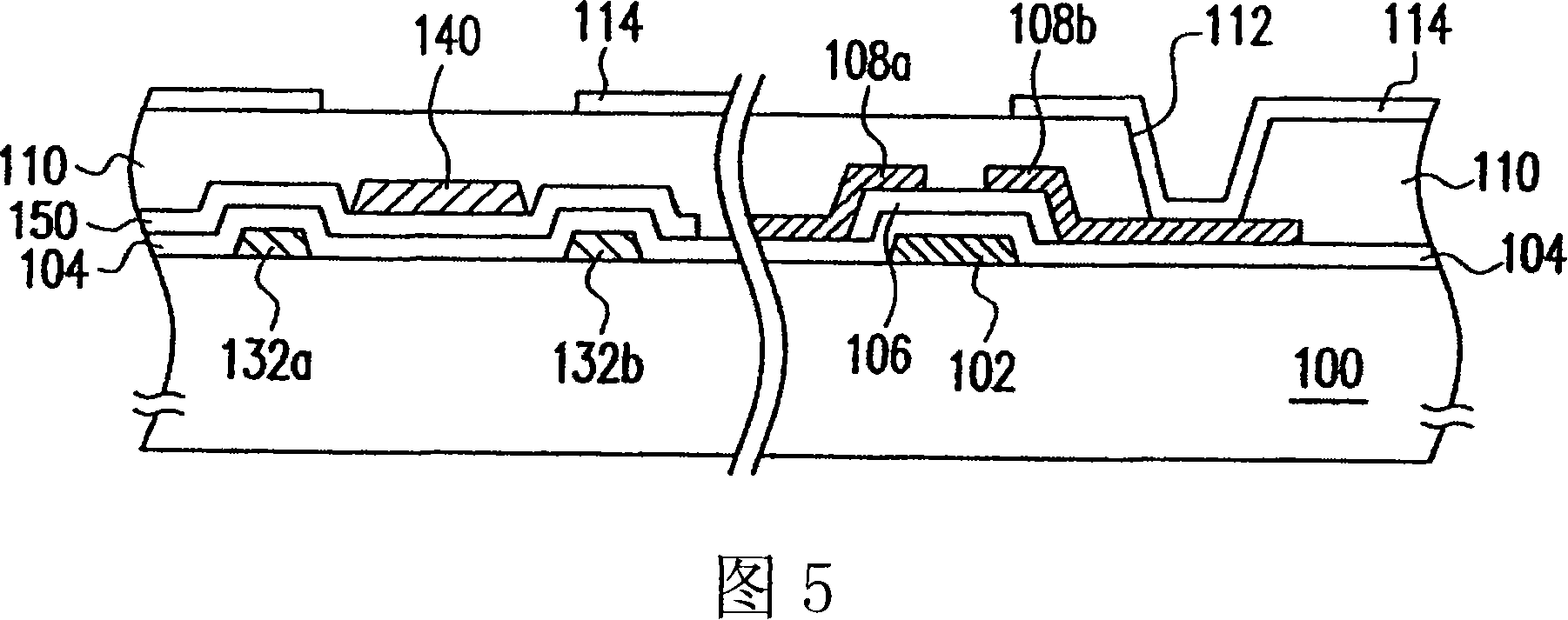
[0045] Another method of manufacturing a pixel structure that can prevent uneven display of the present invention is shown in FIG. 5 , which is a schematic plan view of a pixel structure according to another preferred embodiment of the present invention.

[0046] Referring to FIG. 5 , as previously described in the prior art, when the gate 102 and the scanning wiring 130 are formed on the transparent substrate 100 , the light-shielding layers 132 a and 132 b are also formed on the transparent substrate 100 . After that, a gate insulating layer 104 is formed on the transparent substrate 100 to cover the gate 102 , the scan wiring 130 and the light-shielding layers 132 a and 132 b. Next, a dielectric layer 150 is additionally formed on the gate insulating layer 104 on the light shielding layers 132a and 132b, wherein the material of the dielectric layer 150 is, for example, silicon nitride.

[0047] Next, a channel layer 106 , a source / drain 108 a / 108 b , and a data wiring 140...


PUM


Abstract

The invention discloses a pixel structure and a method for manufacturing the same, in which the pixel structure is suitable to be arranged on a transparent substrate and comprises a scan wiring, a gate insulated layer, a data wiring, shading layers, a thin film transistor, a protective layer, a contact window and a pixel electrode, wherein, the shading layers are arranged on the surface of the transparent substrate, arranged on the two sides of the data wiring and connected electrically with each other to avoid the non-uniform display caused by the inconsistency of the parasitic capacitor of the data wiring and the shading layers on two sides of the data wiring.

Description

[0001] This application is a divisional application based on the Chinese invention patent application titled "Pixel Structure and Manufacturing Method" and application number 02153826.3. technical field [0002] The present invention relates to the structure of a semiconductor component and its manufacturing method, and in particular to a thin film transistor liquid crystal display (Thin Film Transistor Liquid Crystal Display, TFT-LCD) pixel structure and its manufacturing method. Background technique [0003] The TFT liquid crystal display is mainly composed of a TFT array substrate, a color filter array substrate and a liquid crystal layer, wherein the TFT array substrate is composed of a plurality of TFTs arranged in an array, and a pixel electrode corresponding to each TFT (Pixel Electrode). The above thin film transistor includes a gate, a channel layer, a source and a drain, and the thin film transistor is used as a switch component of a liquid crystal display unit. ...

Claims


Application Information

Patent Timeline
Patent Type & Authority Applications(China)
IPC IPC(8): H01L27/12H01L23/522H01L21/84H01L21/768G02F1/1362G02F1/1333G02F1/136H01L29/786
Inventor 黄淑仪陈士元
Owner AU OPTRONICS CORP
Why Eureka
Try Eureka