Electron mobility enhancement for mos devices with nitrided polysilicon re-oxidation

一种半导体、氧化物半导体的技术,应用在半导体器件、半导体/固态器件制造、晶体管等方向,能够解决驱动电流减少、P型金属氧化物半导体性能降低、降低MOS装置性能等问题

Active Publication Date: 2008-05-14
TAIWAN SEMICON MFG CO LTD
View PDF0 Cites 9 Cited by
  • Summary
  • Abstract
  • Description
  • Claims
  • Application Information

AI Technical Summary

Problems solved by technology

[0005] However, the known polysilicon re-oxidation process (polysilicon re-oxidation) brings some adverse effects, such as increasing the channel length and the thickness of the gate dielectric layer, thereby reducing the performance of the MOS device
The reduction in performance includes a reduction in drive current. In order to compensate for the reduction in performance, a nitrided polysilicon re-oxidation process (nitrided polysilicon re-oxidation) can be implemented. In this process, a silicon oxynitride layer is formed to replace the oxide layer. However, the nitrided The polysilicon re-oxidation process is only beneficial for N-type metal oxide semiconductors (NMOS), while the performance of P-type metal oxide semiconductors (PMOS) is reduced

Method used


Image

  • Electron mobility enhancement for mos devices with nitrided polysilicon re-oxidation
  • Electron mobility enhancement for mos devices with nitrided polysilicon re-oxidation
  • Electron mobility enhancement for mos devices with nitrided polysilicon re-oxidation

Examples


Embodiment Construction

[0024] Preferred embodiments according to the present invention will be described below. It must be noted that the present invention provides many applicable inventive concepts, and the specific embodiments disclosed are only illustrative of specific ways to achieve and use the present invention, and are not intended to limit the scope of the present invention.

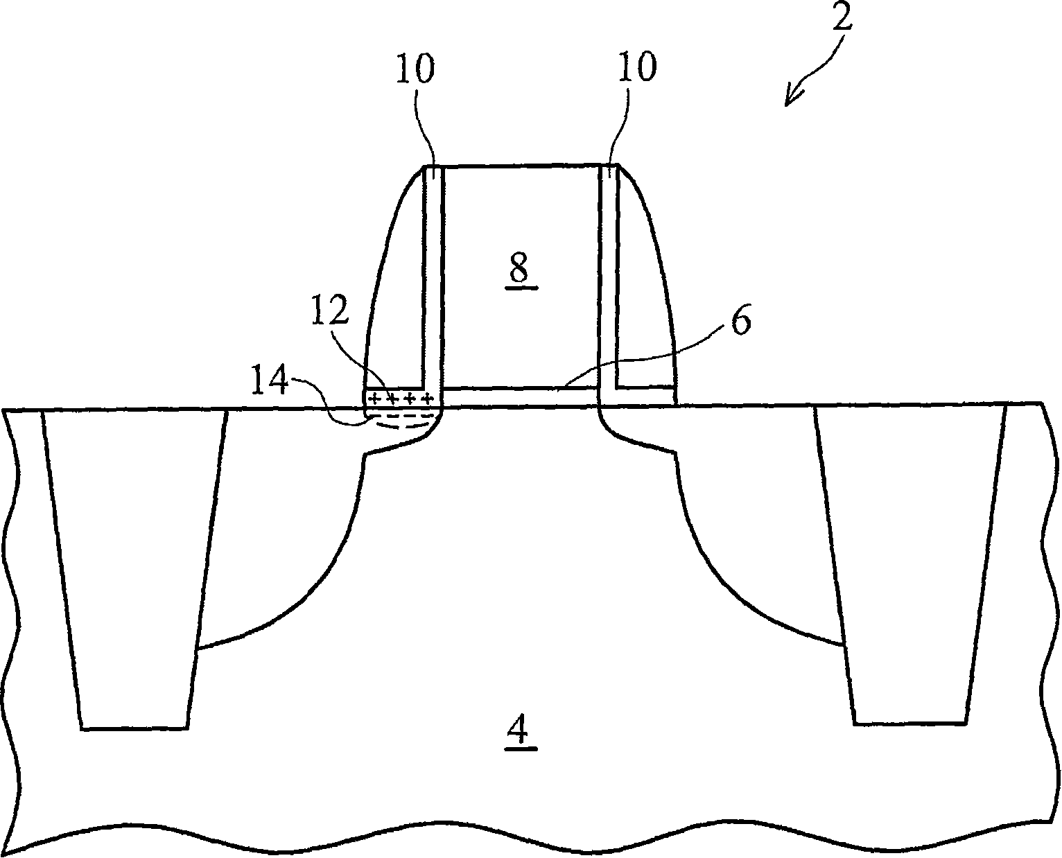
[0025] At present, some studies have found that the nitrided polysilicon re-oxidation process (nitrided polysilicon re-oxidation) is beneficial to NMOS devices, but it degrades the performance of PMOS devices. by figure 1 To explain the possible reasons for this phenomenon, figure 1 A known MOS device is shown in which a MOS device 2 is formed over a silicon substrate 4 . The MOS device 2 includes a gate oxide layer 6 and a polysilicon gate 8 , and a silicon oxynitride layer 10 is formed on the sidewall of the polysilicon gate 8 . The silicon oxynitride layer 10 also includes a horizontal portion 12 above the subst...


PUM


Abstract

A semiconductor structure forming method. The PMOS device includes a first gate dielectric on a semiconductor substrate, a first gate electrode on the first gate dielectric, and a first gate spacer along sidewalls of the first gate electrode and the first gate dielectric. The NMOS device includes a second gate dielectric on the semiconductor substrate, a second gate electrode on the second gate dielectric, a nitrided polysilicon re-oxidation layer having a vertical portion and a horizontal portion wherein the vertical portion is on sidewalls of the second gate electrode and the second gate dielectric and wherein the horizontal portion is on the semiconductor substrate, and a second gate spacer on sidewalls of the second gate electrode and the second gate dielectric, wherein the second gate spacer is on the horizontal portion of the nitrided polysilicon re-oxidation layer.

Description

technical field [0001] The present invention relates to a semiconductor device, and in particular to a structure and a manufacturing method of a metal-oxide-semiconductor (MOS) device. Background technique [0002] Polysilicon gates are often used in the process of metal oxide semiconductor devices. In a typical polysilicon gate process, the gate dielectric layer and the polysilicon layer are first formed, and then the gate dielectric layer and the polysilicon layer are patterned to A gate stack composed of a gate dielectric layer and a gate electrode on the gate dielectric layer is formed. [0003] The patterning process of the gate stack may cause damage to the gate electrode and the gate dielectric layer, thereby affecting the integrity of the gate dielectric layer. One situation that occurs is that there is a high electric field in the region of the gate dielectric adjacent to the bottom of the gate electrode, and the affected gate dielectric will create reliability pro...

Claims


Application Information

Patent Timeline
Patent Type & Authority Applications(China)
IPC IPC(8): H01L27/092H01L21/8238
CPCH01L21/28247H01L21/823864H01L29/66545H01L29/6656
Inventor 林孟竖李达元陈启群陈世昌
Owner TAIWAN SEMICON MFG CO LTD
Why Eureka
Try Eureka