Method of fabricating a semiconductor device having self-aligned floating gate and related device

a floating gate and semiconductor technology, applied in the field of semiconductor devices, can solve the problems of increasing the required integration density of flash memory devices, reducing the size and power consumption of electronic systems, and losing data stored devices

Active Publication Date: 2007-04-26
SAMSUNG ELECTRONICS CO LTD
View PDF7 Cites 305 Cited by
  • Summary
  • Abstract
  • Description
  • Claims
  • Application Information

AI Technical Summary

Benefits of technology

[0012] In one embodiment, the invention is directed to a method of fabricating a flash memory device having a self-aligned floating gate. The method includes forming an isolation layer to define a fin body in a semiconductor substrate. The fin body is formed to have a first sidewall, a second sidewall facing the first sidewall, and a top surface. The fin body also has a portion protruding above the isolation layer. The isolation layer has a sacrificial pattern formed thereon. The sacrificial pattern has an opening self-aligned with the protruding portion of the fin bod

Problems solved by technology

Volatile memory devices lose data stored in them when power is cut off, while nonvolatile memory devices retain stored data even when the power is cut off.
Meanwhile, as the size and power consumption of electronic systems are gradually red

Method used


Image

  • Method of fabricating a semiconductor device having self-aligned floating gate and related device
  • Method of fabricating a semiconductor device having self-aligned floating gate and related device
  • Method of fabricating a semiconductor device having self-aligned floating gate and related device

Examples


first embodiment

[0020] A method of fabricating a memory device according to the present invention will now be described with reference to FIGS. 1 to 11.

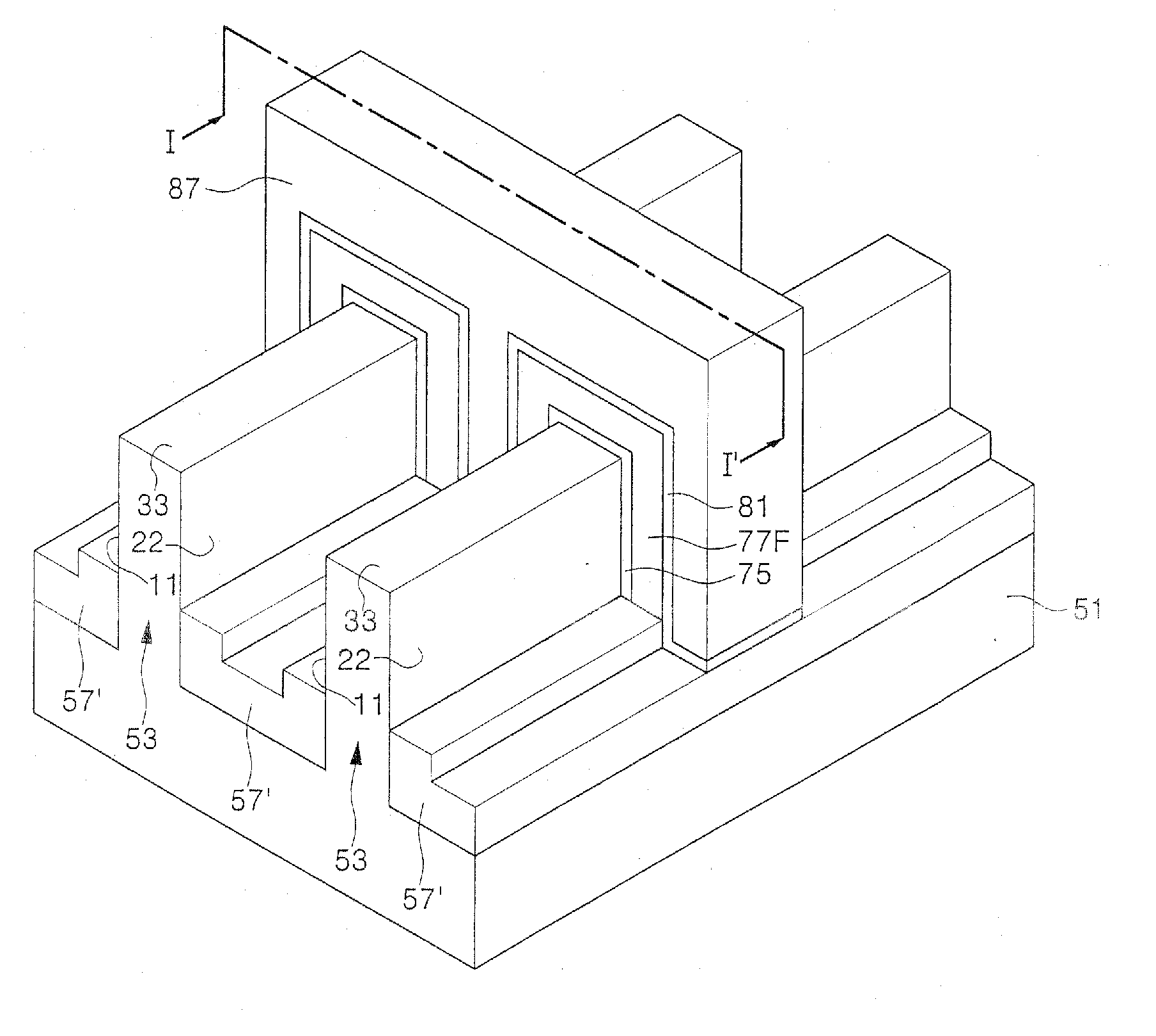
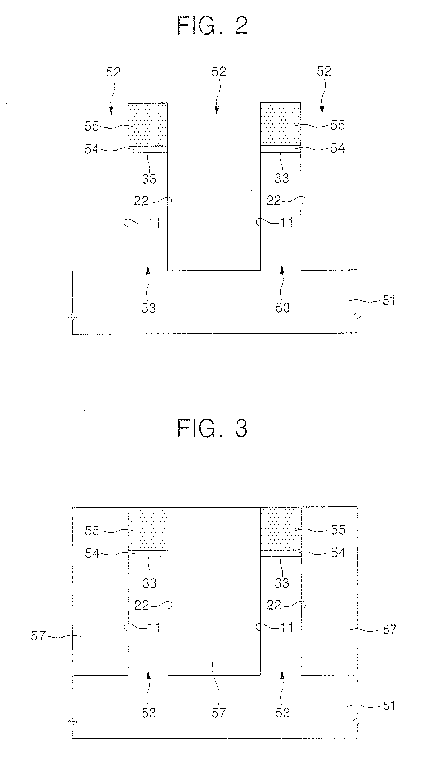
[0021] Referring to FIGS. 1 and 2, a trench 52 defining a fin body 53 is formed in a predetermined region of a semiconductor substrate 51.

[0022] Specifically, a mask layer may be formed on the semiconductor substrate 51. The mask layer may be patterned to expose the predetermined region of the semiconductor substrate 51; thus forming a hard mask pattern 55. The semiconductor substrate 51 may be a silicon wafer. The hard mask pattern 55 may comprise a nitride layer, such as a silicon nitride layer, by a chemical vapor deposition (CVD) method.

[0023] Before the mask layer is formed, a pad oxide layer 54 may be formed on the semiconductor substrate 51. The pad oxide layer 54 may comprise a thermal oxide layer. The pad oxide layer 54 may release physical stress due to a difference in thermal expansion coefficient between the semiconductor substrate 51 ...

second embodiment

[0048] Now, a method of fabricating a flash memory device according to the present invention will be described with reference to FIGS. 12 to 19.

[0049] Referring to FIGS. 12 and 13, a fin body 53, a pad oxide layer 54, a hard mask pattern 55, an isolation layer 57′, a sacrificial oxide layer 61, and a sacrificial spacer layer 63 are formed on a semiconductor substrate 51, as in the method of fabricating the flash memory device according to the first embodiment of the present invention.

[0050] The sacrificial spacer layer 63 may be anisotropically etched to form a sacrificial spacer 63′ that covers sidewalls of the hard mask pattern 55 and first and second sidewalls 11 and 22 of the fin body 53. The process of anisotropically etching the sacrificial spacer layer 63 may be performed until the isolation layer 57′ is exposed in the trench 52. In this case, a top surface of the hard mask pattern 55 may also be exposed.

[0051] Referring to FIGS. 12 and 14, a sacrificial layer may be formed...


PUM


Abstract

A semiconductor device such as a flash memory device having a self-aligned floating gate and a method of fabricating the same is provided. An embodiment of the device includes an isolation layer defining a fin body is formed in a semiconductor substrate. The fin body has a portion protruding above the isolation layer. A sacrificial pattern is formed on the isolation layer. The sacrificial pattern has an opening self-aligned with the protruding portion of the fin body. The protruding fin body is exposed in the opening. An insulated floating gate pattern is formed to fill the opening. The sacrificial pattern is then removed. An inter-gate dielectric layer covering the floating gate pattern is formed. A control gate conductive layer is formed over the inter-gate dielectric layer. The control gate conductive layer, the inter-gate dielectric layer, and the floating gate pattern are patterned to form a control gate electrode crossing the fin body as well as the insulated floating gate interposed between the control gate electrode and the fin body.

Description

CROSS-REFERENCE TO RELATED APPLICATION [0001] This application claims priority to and the benefit of Korean Patent Application No. 2005-0101509, filed Oct. 26, 2005, which is incorporated herein by reference in its entirety. BACKGROUND [0002] 1. Field of the Invention [0003] The present invention relates to a semiconductor device such as a nonvolatile memory device and a method of fabricating the same, and more particularly, to a flash memory device having a self-aligned floating gate and a method of fabricating the same. [0004] 2. Description of the Related Art [0005] In general, semiconductor memory devices storing data can be classified into volatile memory devices and nonvolatile memory devices. Volatile memory devices lose data stored in them when power is cut off, while nonvolatile memory devices retain stored data even when the power is cut off. Accordingly, nonvolatile memory devices, such as flash memory devices, are widely used in mobile storage devices, mobile telecommuni...

Claims


Application Information

Patent Timeline
IPC IPC(8): H01L21/336
CPCH01L21/84H01L27/115H01L27/11521H01L27/1203H01L29/66795H01L29/7851H10B69/00H10B41/30H01L21/823468
Inventor CHOI, BYUNG-YONGLEE, CHOONG-HOKIM, TAE-YONGPARK, DONG-GUN
Owner SAMSUNG ELECTRONICS CO LTD
Why Eureka
Try Eureka