Process for depositing electrode with high effective work function

a high-efficiency, electrode-deposited technology, applied in the direction of basic electric elements, electrical equipment, semiconductor devices, etc., can solve the problems of poor performance characteristics of transistors with high-k materials

Active Publication Date: 2015-09-15
ASM IP HLDG BV
View PDF26 Cites 325 Cited by
  • Summary
  • Abstract
  • Description
  • Claims
  • Application Information

AI Technical Summary

Problems solved by technology

Transistors with these high-k materials, however, may have poor performance characteristics when the high-k materials are used with some traditional silicon-based gate electrode materials.

Method used


Image

  • Process for depositing electrode with high effective work function
  • Process for depositing electrode with high effective work function
  • Process for depositing electrode with high effective work function

Examples


example 1

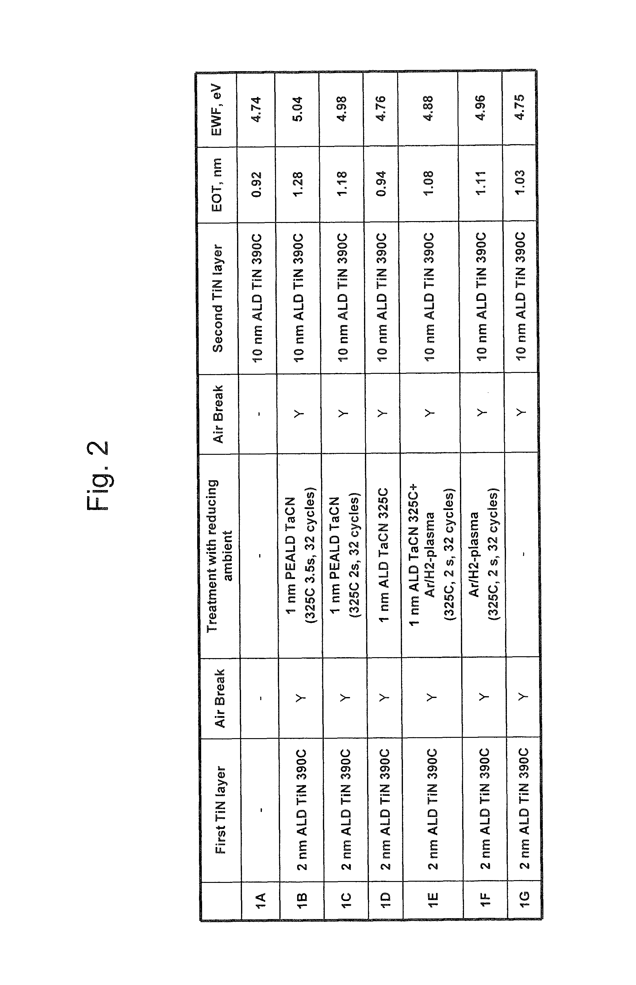
[0058]Example 1 will be discussed with reference to FIGS. 9a-9c. The gate dielectric may include HfO2. From bottom to top, the PMOS metal electrode is formed by deposition of a 2 nm TiN layer, a 1 nm TaCN layer, a 4 nm TiN layer, a 5 nm TiAl layer and a layer of fill metal. The NMOS metal electrode includes, from bottom to top, a 2 nm TiN layer, a 1 nm TaCN layer, a 5 nm TiAl layer, and a layer of fill metal. TiAl provides a low work function for NMOS. In the PMOS stack, however, the TiAl layer is remote from the HfO2 / metal electrode interface and has limited influence on the PMOS stack work function at that HfO2 / metal electrode interface. The treatment with Ar / H* (where H* indicates an excited-hydrogen containing species, such as hydrogen radicals in a plasma) in the PMOS stack can be applied before the TaCN layer deposition (FIGS. 9a and 9b), during the TaCN deposition if a plasma enhanced deposition process is used to form the TaCN layer (FIG. 9c), or after the TaCN layer deposit...

example 2

[0088]Example 2 will be discussed with reference to FIG. 10. The gate dielectric layer may include HfO2. The PMOS metal electrode is formed by deposition of a 2 nm TiN layer, treatment of the TiN layer by a hydrogen containing gas, deposition of a 4 nm TiN layer, and deposition of a fill metal. The NMOS metal electrode includes a first 2 nm TiN layer, a 5 nm TiAl layer, a 4 nm second TiN layer and a fill metal layer. The stacks of FIG. 10 can be produced using the following process flow:[0089]1. Deposition of a first TiN layer and a TiAl layer;[0090]2. Lithography and etch to form a protection layer (e.g. a photo resist layer or SiO2 layer) on NMOS devices;[0091]3. Remove the TiAl layer from PMOS devices, with etch stop on the TiN layer;[0092]4. Treatment in a hydrogen-containing gas;[0093]5. Removal of the protection layer; and[0094]6. Deposition of a second TiN layer and a fill metal.

example 3

[0095]Example 3 will be discussed with reference to FIG. 11. The PMOS electrode is formed by deposition of a 2 nm TiN layer, treatment of the TiN layer in a hydrogen-containing gas, deposition of a 5 nm TaC layer, and deposition of a fill metal layer. The NMOS stack may include a 5 nm TaC layer, and a layer of fill metal. TaC also provides a low work function, suitable for NMOS devices, and comparable to TiAl. However, TaC has the advantage that it can be deposited by ALD whereas TiA1 is typically formed by a PVD process. The stacks of FIG. 11 can be produced by the following process sequence:[0096]1. Deposition of a first TiN layer;[0097]2. Treatment in a hydrogen-containing gas;[0098]3. Lithography and etch (optionally, with a SiO2 hardmask) to remove TiN from NMOS devices, with etch stop on HfO2;[0099]4. (Optional hardmask removal, if applicable);[0100]5. Deposition of a TaC layer to set EWF of NMOS devices; and[0101]6. Deposition of fill metal.


PUM

PropertyMeasurementUnit
work functionaaaaaaaaaa
peak-to-peak voltageaaaaaaaaaa
thicknessaaaaaaaaaa

Abstract

According to some embodiments, an electrode have a high effective work function is formed. The electrode may be the gate electrode of a transistor and may be formed on a high-k gate dielectric by depositing a first layer of conductive material, exposing that first layer to a hydrogen-containing gas, and depositing a second layer of conductive material over the first layer. The first layer may be deposited using a non-plasma process in which the substrate is not exposed to plasma or plasma-generated radicals. The hydrogen-containing gas to which the first layer is exposed may include an excited hydrogen species, which may be part of a hydrogen-containing plasma, and may be hydrogen-containing radicals. The first layer may also be exposed to oxygen before depositing the second layer. The work function of the gate electrode in the gate stack may be about 5 eV or higher in some embodiments.

Description

PRIORITY APPLICATION[0001]This disclosure claims the benefit under 35 U.S.C. §119(e) of U.S. Provisional Patent Application No. 61 / 492,207, filed Jun. 1, 2011, entitled “PROCESS FOR DEPOSITING ELECTRODE WITH HIGH EFFECTIVE WORK FUNCTION,” and assigned to the assignee hereof. The disclosure of the prior application is incorporated by reference herein in its entirety.TECHNICAL FIELD[0002]This disclosure relates to the field of semiconductor processing and, more particularly, to the deposition of conductive structures, such as metal gate electrodes, including metal gate electrodes in gate stacks in transistors.DESCRIPTION OF THE RELATED ART[0003]Due to continual demands for increased computing power and decreased integrated circuit sizes, there is also a continual demand to decrease the sizes of the electronic devices that form the integrated circuits. For example, the sizes of transistors continue to be reduced in order to, e.g., increase the density of the transistors in an integrate...

Claims


Application Information

Patent Timeline
Patent Type & Authority Patents(United States)
IPC IPC(8): H01L21/8238H01L29/66H01L29/49H01L21/28H01L29/78
CPCH01L29/66545H01L21/823842H01L21/28088H01L29/4966H01L29/7833
Inventor MACHKAOUTSAN, VLADIMIRMAES, JAN WILLEMXIE, QI
Owner ASM IP HLDG BV
Why Eureka
Try Eureka