SOI stacked DRAM logic

a logic and stacking technology, applied in semiconductor/solid-state device testing/measurement, semiconductor device details, semiconductor/solid-state device testing/measurement, etc., can solve the problem of incompatibility of soi transistors and trench capacitors, large chip area and other issues, to achieve the effect of avoiding the formation of memory cells

Inactive Publication Date: 2003-04-08
INT BUSINESS MASCH CORP
View PDF20 Cites 426 Cited by
  • Summary
  • Abstract
  • Description
  • Claims
  • Application Information

AI Technical Summary

Benefits of technology

It is a further object of the invention to provide a layered semiconductor chip where the length of connections between devices in respective layers can be minimized and provided over any or all regions of the chip.
It is another further object of the invention to provide a technique of forming a semiconductor integrated circuit device in which arbitrary circuit elements can be formed consistent with a restricted heat budget for gate oxides of high performance field effect transistors.
In accordance with another aspect of the invention, a method of forming a semiconductor integrated circuit is provided comprising steps of forming integrated circuit elements in a first wafer, forming an oxide layer over the circuit elements, bonding a second wafer to the oxide layer, forming integrated circuit elements at a surface of the second wafer, and forming connections from the integrated circuit elements in the second wafer to the integrated circuit elements in the first wafer. In this way, interchip connections between wafers can be lithographically defined and reliably formed in much increased numbers at pitches similar to intrachip connection pitches.

Problems solved by technology

However, the support circuitry requires substantial chip area which is thus not available for formation of memory cells.
However, SOI transistors and trench capacitors are not compatible and cannot be easily integrated on the same chip.
Further, the active device layer of SOI wafers is too thin to provide adequate capacitance at currently feasible minimum lithographic feature sizes and forming a trench through the insulator of an SOI wafer or chip would compromise the electrical isolation thereof.
Moreover, the thermal budget required to form trench capacitors and node interconnections greatly exceeds the desired heat budget for forming high speed, low voltage logic switching devices in SOI.
Another problem involving on-chip capacitances required in increasing numbers of types of integrated circuits is the decoupling capacitance which is required in logic circuits operating at low voltage and clock frequencies greater than about 400 MHz to prevent unacceptable levels of switching noise (relative to the operating voltage) from being propagated through power connections.
The intrachip area required for a planar capacitor is so large that multiple power supplies to reduce power / performance trade-offs cannot be included on the chip since the voltage regulators cannot be adequately decoupled with the capacitors which can be provided.
However, when chips are stacked, interchip connections other than at edges of the chips cannot be reliably formed at minimum lithography feature size and the available area of the edges limits the number of connections which can be made.
For both of these reasons, the number of interchip connections that can be reliably formed and used is very limited and is certainly insufficient for memory capacities which can be foreseen.
Connections at the edges of chips are also not optimally short to limit signal propagation time.
Accordingly, there has been no solution to providing transistors of improved performance on the same chip with trench capacitor arrays while the need for faster access time and larger numbers of storage cells and high speed logic for accessing them has not been fully answered using technologies which are compatible with each other or incompatible technologies on separately processed, commonly packaged chips.
Therefore, the current state of the art does not support significant further increases in either memory capacity or performance and requires substantial processing to both align the chip faces and seal the interchip wiring from external atmosphere which could cause deterioration thereof.

Method used


Image

  • SOI stacked DRAM logic
  • SOI stacked DRAM logic
  • SOI stacked DRAM logic

Examples


second embodiment

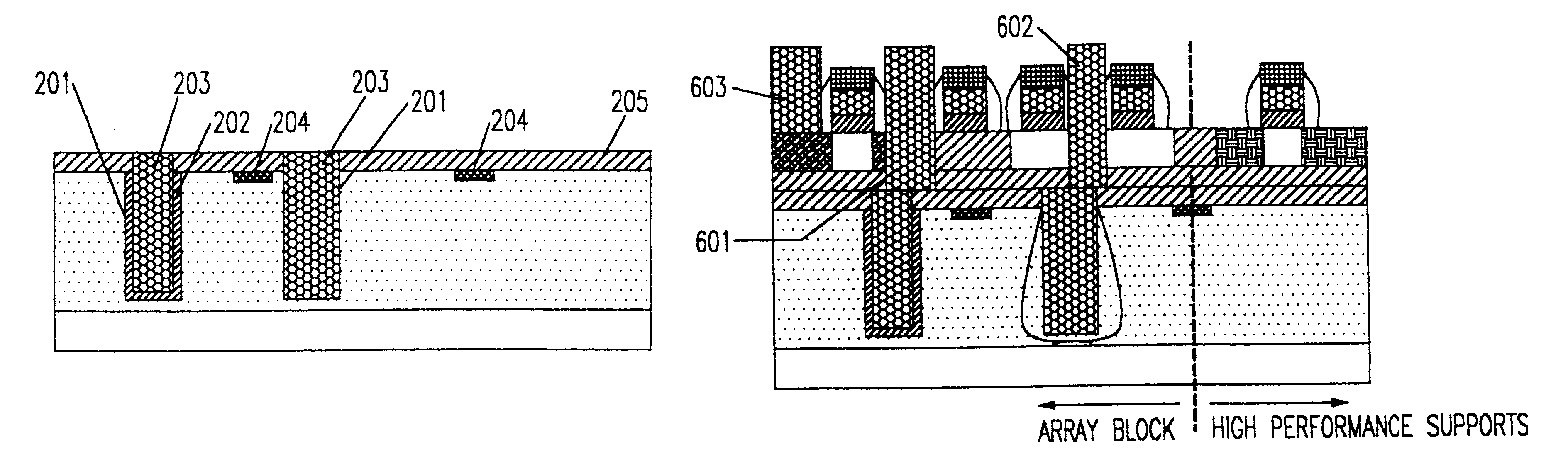
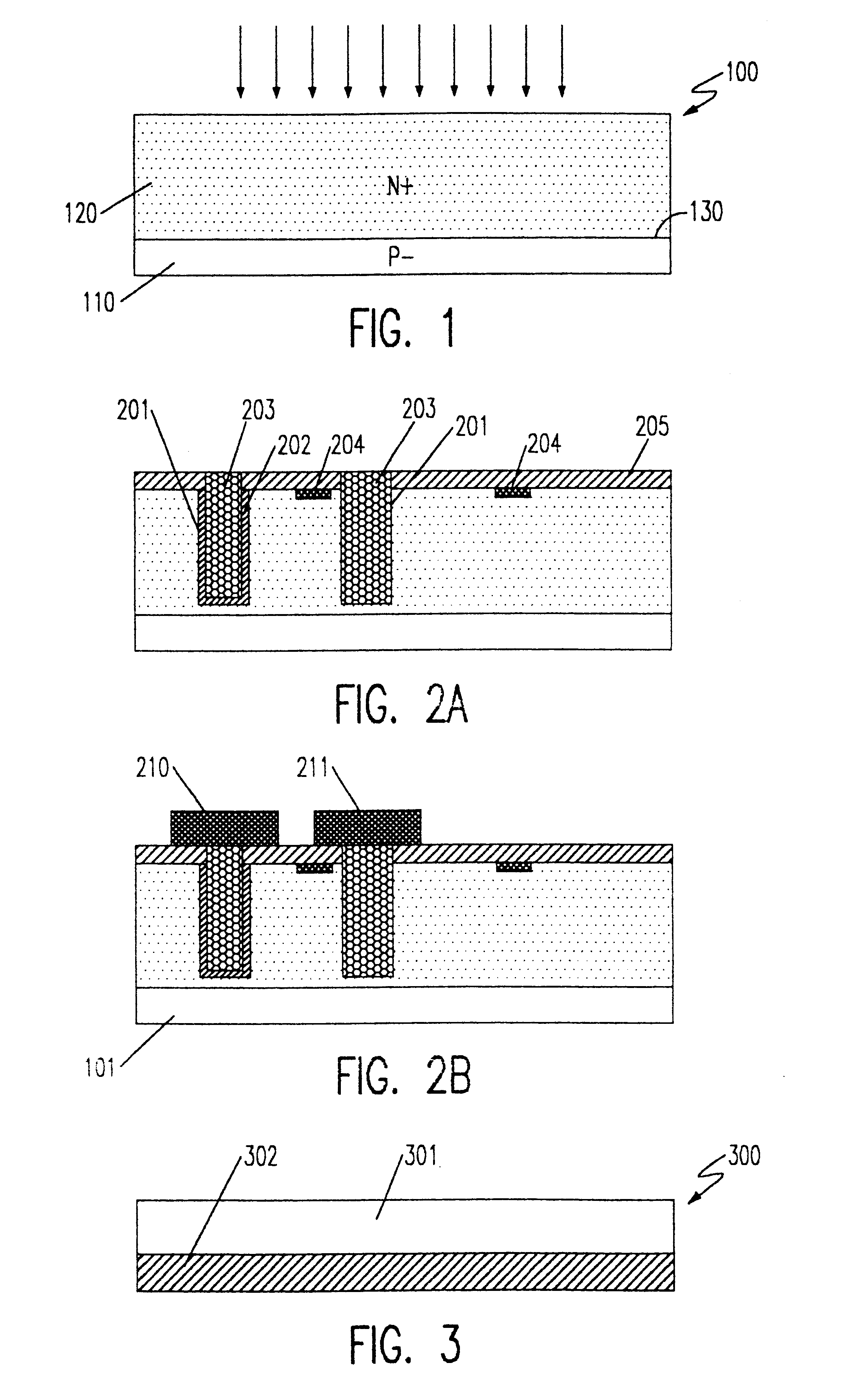
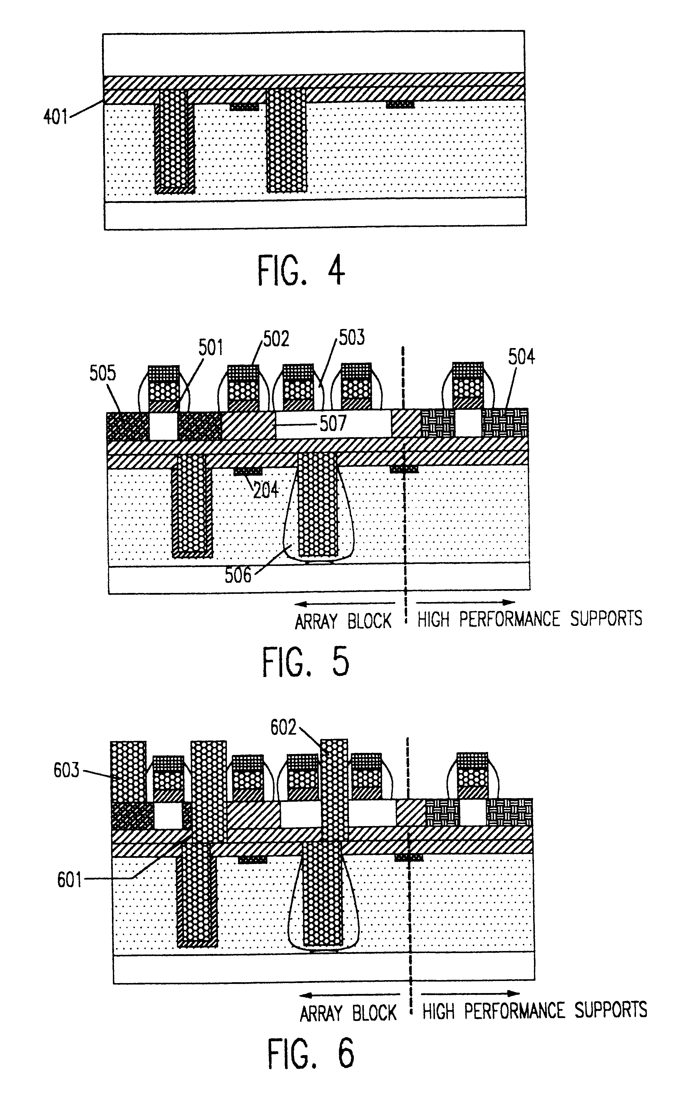
the invention will now be described with reference to FIGS. 7-11. FIG. 7 shows a wafer at a stage of fabrication similar to that of FIG. 2A, described above and formed in substantially the same manner. However, FIG. 7 differs from FIG. 2A by inclusion of support devices 701 and array devices 702 which can be formed on the same substrate by processes compatible with the formation of the memory cell array. Alignment marks 204 are provided as described above. Additionally, while connections within and between the array and support sections, it will generally be found convenient to provide connection pads 703, 704 at the surface 705 of a planarized insulator (passivation) layer.

As shown in FIG. 8, an insulator / oxide 801 is deposited and a SOI wafer is bonded thereto by processes such as those described above as shown in FIG. 9. High performance devices can then be formed on and / or in the SOI active layer and connections 901 formed to connection pads 703 (and / or 704) in the manner descri...


PUM


Abstract

A composite, layered, integrated circuit formed by bonding of insulator layers on wafers provides for combination of otherwise incompatible technologies such as trench capacitor DRAM arrays and high performance, low power, low voltage silicon on insulator (SOI) switching transistors and short signal propagation paths between devices formed on respective wafer layers of a chip. In preferred embodiments, an SOI wafer is formed by hydrophilic bonding of a wafer over an integrated circuit device and then cleaving a layer of the second wafer away using implanted hydrogen and low temperature heat treatment. Further wafers of various structures and compositions may be bonded thereover and connections between circuit elements and connection pads in respective wafers made using short vias that provide fast signal propagation as well as providing more numerous connections than can be provided on chip edges.

Description

1. Field of the InventionThe present invention generally relates to semiconductor integrated circuits and, more particularly, to high capacity dynamic random access memories including high performance transistors in support circuitry thereof and other types of devices having differing circuit element requirements and to testing and burn-in thereof.2. Description of the Prior ArtAs the processing power of microprocessors has increased and cycle times reduced, higher capacity memories with more rapid access time have been demanded. Accordingly, dynamic memories have been developed with storage cells requiring reduced area or footprint such that memory chips having a capacity of a gigabit or more can be foreseen. Such storage cells are often formed by lining trenches in a chip of doped semiconductor with an insulator and filling the remainder of the trench with doped polysilicon to form an array of capacitors having a common electrode formed by the chip. A storage cell of such an array...

Claims


Application Information

Patent Timeline
Patent Type & Authority Patents(United States)
IPC IPC(8): H01L21/768H01L21/70H01L27/12H01L21/8242H01L23/58H01L27/108H01L23/48
CPCH01L21/76838H01L21/76895H01L23/481H01L27/10867H01L27/1203H01L2924/0002H01L22/32H01L27/10832Y10S977/90Y10S977/779Y10S977/712Y10S977/721Y10S977/94H01L2924/00H01L23/535H10B12/373H10B12/0385
Inventor DIVAKAUNI, RAMACHANDRAHAKEY, MARK C.MA, WILLIAM H.-L.MANDELMAN, JACK A.TONTI, WILLIAM R.
Owner INT BUSINESS MASCH CORP
Why Eureka
Try Eureka