Control circuit and display device

a control circuit and display device technology, applied in the field of electronic technology, can solve the problems of non-uniform display image of the display device, and achieve the effects of uneven display brightness of the entire pixel array, increased connection resistance, and longer connection lines

Active Publication Date: 2017-04-06
WUHAN CHINA STAR OPTOELECTRONICS TECH CO LTD
View PDF0 Cites 5 Cited by
  • Summary
  • Abstract
  • Description
  • Claims
  • Application Information

AI Technical Summary

Benefits of technology

[0020]The driver of the present invention needs to charge each row pixels of the pixel array. Because the pixel array comprises a plurality of rows of pixels, the plurality of rows of pixels are sequentially aligned in a form of array to be arranged under the driver. The distances of the different rows of pixels with the driver are different. The lengths of the connection lines of the driver with each row pixels are different. Meanwhile, with the distance between the row of the pixels and the driver gets larger and larger, the length of the connection line of the driver with the corresponding row of the pixels also gets longer and longer. The longer the connection is, the larger the connection resistance is, too. Thus, the charging quantity of the driver to the corresponding row of pixels is smaller. Consequently, the charge quantity to the entire pixel array is not even. The display brightness of the entire pixel array becomes uneven. The drive control circuit of the present invention comprises a resistor. The driver is coupled to the N columns pixels of the pixel array through the resistor to charge the N columns pixels. The resistor comprises a first resistor and a second resistor. An area surrounded by the pixel array is divided into a first area and a second area. Both the first area and the second area comprise at least one row pixels. A length of a connection line of the driver with any row pixels in the first area is smaller than a length of a connection line of the driver with any row pixels in the second area. When the driver determines that it is required to sequentially supply power to each row pixels of the first area, the first resistor is activated to make a power supply signal outputted by the driver pass through the first resistor and be sequentially outputted to each row pixels of the first area for sequentially supplying power to the each row pixels of the first area. When the driver determines that it is required to sequentially supply power to each row pixels of the second area, the second resistor is activated to make the power supply signal outputted by the driver pass through the second resistor and be sequentially outputted to each row pixels of the second area for sequentially supplying power to the each row pixels of the second area. Because the resistance of the first resistor is larger than the resistance of the second resistor, the first total resistance (a sum of the corresponding line resistance and the first resistor) of the lines of the driver with the pixels in the first area and the second total resistance (a sum of the corresponding line resistance and the second resistor) of the lines of the driver with the pixels in the second area are balanced. Thus, the charge quantity of the driver to the corresponding row pixels is balanced. Therefore, the display brightness of the entire pixel array is balanced.

Problems solved by technology

Because the voltage charge quantity of the liquid crystal unit varies with the change of the connection line resistance, the display image of the display device has nonuniform defects.

Method used


Image

  • Control circuit and display device
  • Control circuit and display device
  • Control circuit and display device

Examples


Embodiment Construction

[0025]For better explaining the technical solution and the effect of the present invention, the present invention will be further described in detail with the accompanying drawings in the specific embodiments.

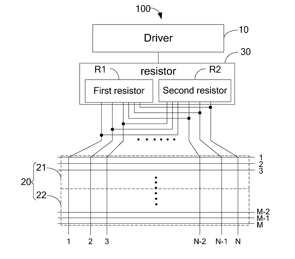
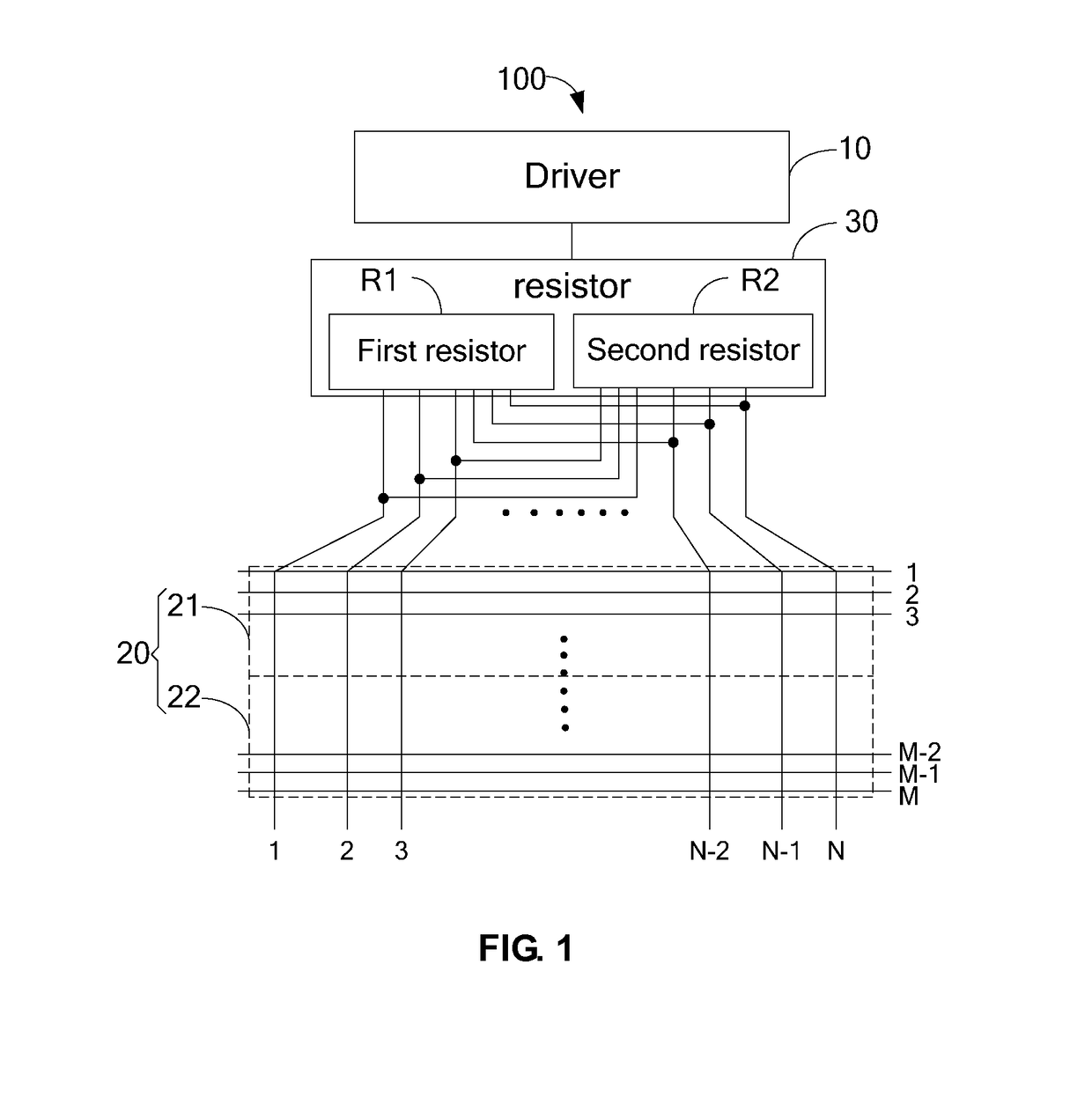
[0026]Please refer to FIG. 1. The first embodiment of the first solution according to the present invention provides a drive control circuit 100. The drive control circuit 100 comprises a driver 10, a pixel array 20 and a resistor 30. The pixel array 20 comprises M×N pixels (not shown) aligned in a form M rows×N columns, wherein M is a natural number larger than 1, and N is a natural number. The driver 10 is coupled to the N columns pixels of the pixel array 20 through the resistor 30 to charge the N columns pixels. The resistor 30 comprises a first resistor R1 and a second resistor R2. A resistance of the first resistor R1 is larger than a resistance of the second resistor R2. An area surrounded by the pixel array 20 is divided into a first area 21 and a second area 22. Both t...


PUM


Abstract

Disclosed is a drive control circuit, comprising a driver, a pixel array and a resistor, and the pixel array comprises M×N pixels, and M is a natural number larger than 1, and N is a natural number, and the driver is coupled to the N columns pixels through the resistor, and the resistor comprises a first resistor and a second resistor, and a resistance of the first resistor is larger than a resistance of the second resistor, and an area surrounded by the pixel array is divided into a first area and a second area, and the first area and the second area comprise at least one row pixels, and a length of a connection line of the driver with any row pixels in the first area is smaller than a length of a connection line of the driver with any row pixels in the second area.

Description

CROSS REFERENCE[0001]This application claims the priority of Chinese Patent Application No. 201510229355.2, entitled “Control circuit and display device”, filed on May 7, 2015, the disclosure of which is incorporated herein by reference in its entirety.FIELD OF THE INVENTION[0002]The present invention relates to an electronic technology field, and more particularly to a control circuit and a display device.BACKGROUND OF THE INVENTION[0003]In display devices, the connection lines are formed among the output channels of the source driver and the data lines of the pixel array for respectively coupling the output channels of the source driver with the data lines. The data signal outputted by the output channels of the source driver is transmitted from the first row to the last row of the pixel array. The connection line is longer, and the resistance of the line is larger. The voltage charge quantity of the liquid crystal units in the pixel array changes according to the resistances of t...

Claims


Application Information

Patent Timeline
Patent Type & Authority Applications(United States)
IPC IPC(8): G09G3/36
CPCG09G2320/0233G09G3/3688G09G2300/0426G09G2320/0223
Inventor TANG, YUEJUN
Owner WUHAN CHINA STAR OPTOELECTRONICS TECH CO LTD
Why Eureka
Try Eureka