Method of depositing dielectric film by modified peald method

a dielectric film and modified peal technology, applied in chemical vapor deposition coating, coating, metallic material coating process, etc., can solve the problems of poor conformality or poor step coverage on a substrate containing small features, poor conformal coverage hampering the development of higher density circuit devices and elements, and extremely poor deposition rate. , to achieve the effect of high conformality, high deposition rate and high conformality

Active Publication Date: 2012-08-30
ASM JAPAN
View PDF1 Cites 425 Cited by
  • Summary
  • Abstract
  • Description
  • Claims
  • Application Information

AI Technical Summary

Benefits of technology

[0007]Embodiments of the present invention provide a method of forming thin films using modified plasma enhanced atomic layer deposition (PEALD) at low temperatures (under 600° C., particularly under 400° C.) at high deposition rates with high conformality (e.g., at least 90%). Furthermore, the present invention provides a method for modifying etch properties (such as etching rate) of the deposited layers by adding a second precursor while maintaining a high deposition rate and high conformality.
[0008]Accordingly, in an aspect, an object of at least one embodiment of the present invention is to provide a method of forming a highly conformal (e.g., at least 90%, in some embodiments, no less than 95%) layer, such as a layer of silicon nitride, on surfaces of trenches for an integrated circuit at low temperatures (e.g., <400° C.), and as explained below, one or more of the disclosed embodiments effectively accomplish at least the object.
[0011]In another aspect, an object of at least one embodiment of the present invention is to provide a method for modifying etch properties of a layer, such as a layer of silicon nitride, which has a high conformal (step coverage 90% or higher, in some embodiments, no less than 95%) layer on surfaces of trenches for an integrated circuit at low temperatures (e.g., <600° C.), and as explained below, one or more of the disclosed embodiments effectively accomplish at least the object.

Problems solved by technology

However, the PECVD methods for forming silicon nitride lead to poor conformality or poor step coverage on a substrate containing small features.
In a small circuits and devises such as ultra-large scale integrated (ULSI) circuitries, such poor conformal coverage hampers the development of higher density circuit devices and elements.
However, the ALD or PEALD methods for forming silicon nitride lead to extremely poor deposition rates.
Such poor deposition rates hamper lowering the manufacturing cost for development of higher density circuit devices and elements.

Method used


Image

  • Method of depositing dielectric film by modified peald method
  • Method of depositing dielectric film by modified peald method
  • Method of depositing dielectric film by modified peald method

Examples


example 2

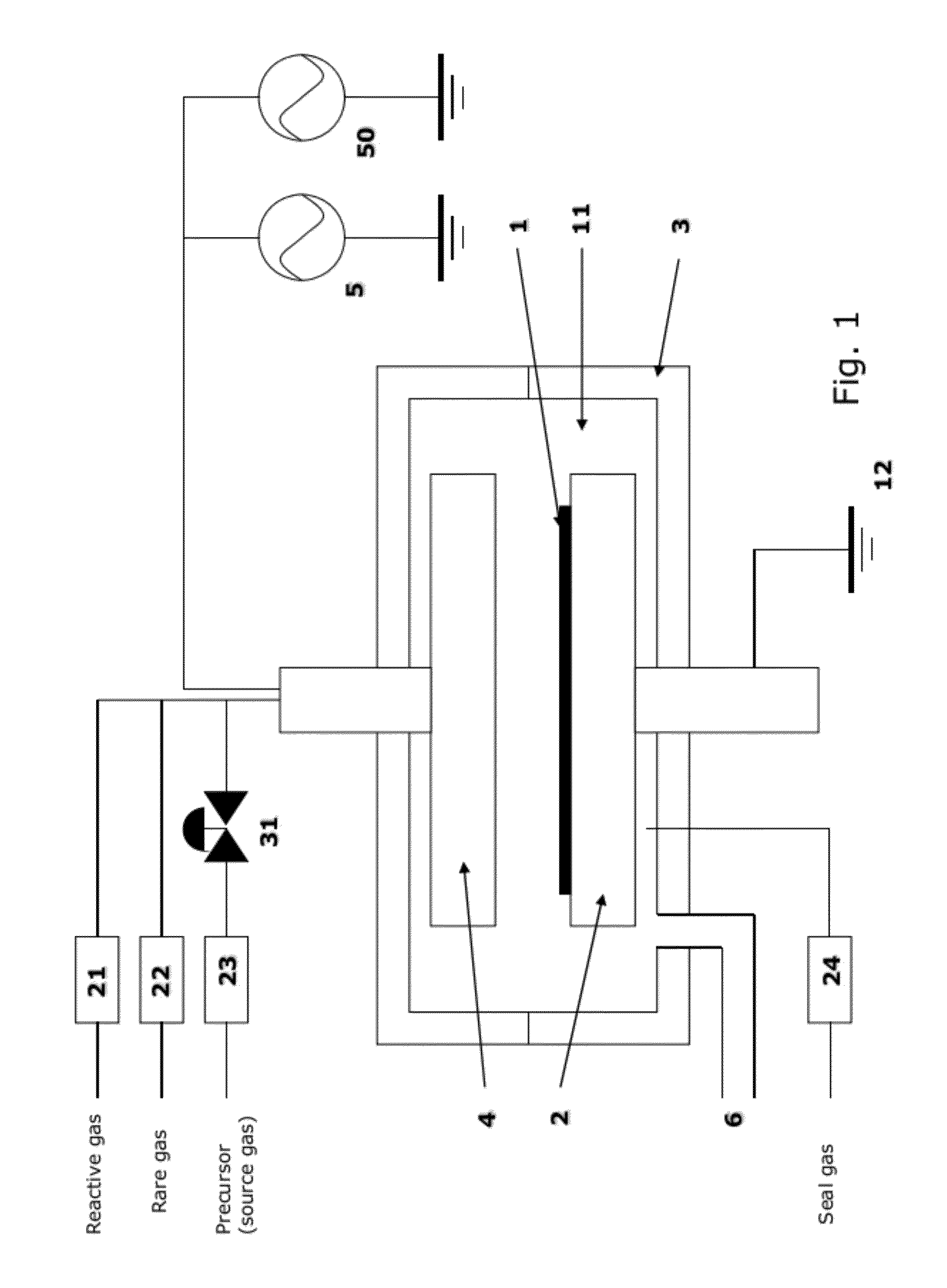
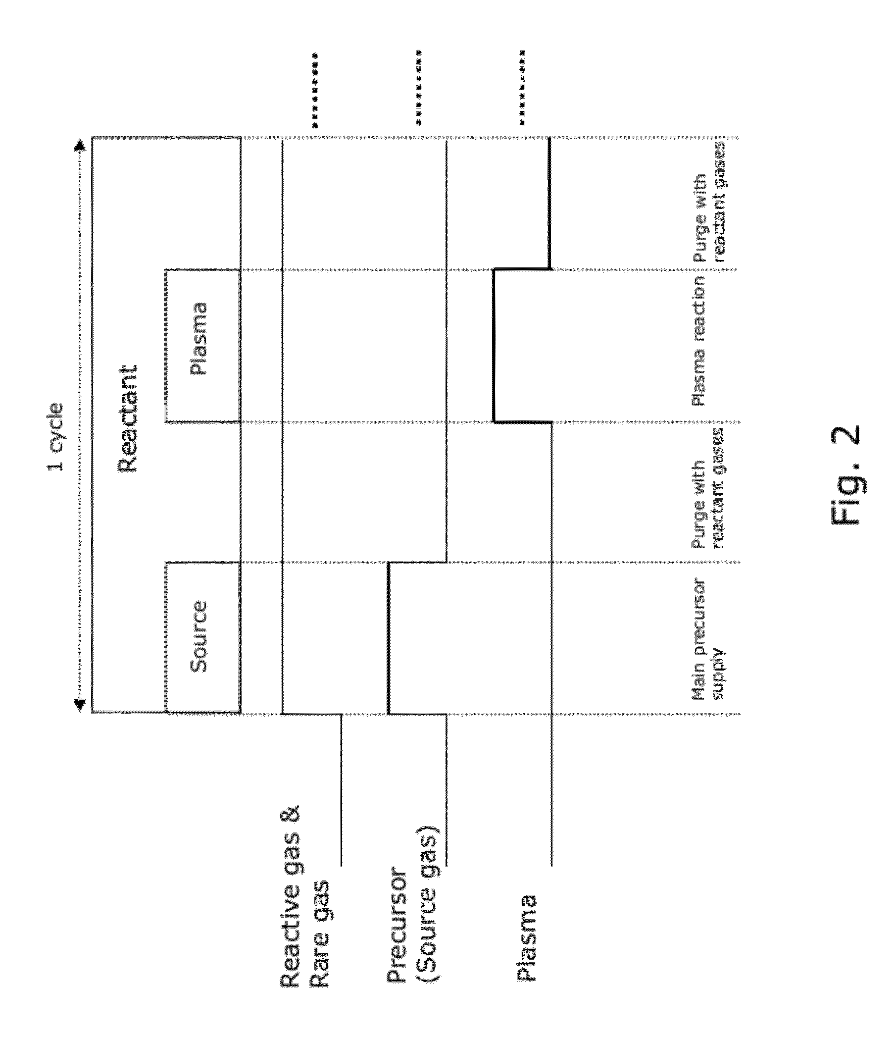
[0112]A dielectric layer having Si—N bonds was formed on a substrate under the condition shown below using the sequence illustrated in FIG. 3 and the PEALD apparatus illustrated in FIG. 1.

[0113]Trisilylamine: 100 sccm

[0114]Hydrogen: 500 sccm

[0115]Nitrogen: 1000 sccm

[0116]Process helium: 1400 sccm

[0117]Sealed helium: 500 sccm

[0118]Argon: 500 sccm

[0119]Substrate temperature: 350° C.

[0120]High frequency RF power (a frequency of 13.56 MHz): 0.07 W / cm2

[0121]Low frequency RF power (a frequency of 430 kHz): 0.0 W / cm2

[0122]Trisilylamine supply time: 1.0, 0.7, 0.5, and 0.1 sec supply

[0123]RF Plasma exciting time: 1.0 sec excite

[0124]Purge time: 1.0 sec interval with reactive gases

[0125]FIG. 4 shows film thickness per cycle of the comparative PEALD method and the disclosed embodiments of the present invention method. In case of the disclosed embodiments (immediate RF plasma), the film thickness per cycle is approximately 0.17˜0.19 nm / cycle as shown in line “b” (1.0 sec pulse of precursor su...

example 3

[0129]A dielectric layer having Si—N bonds was formed with second precursor, for example ammonia, on a substrate under the condition shown below using the sequence illustrated in FIG. 2 and the PEALD apparatus illustrated in FIG. 1.

[0130]Trisilylamine: 100 sccm

[0131]Hydrogen: 500 sccm

[0132]Nitrogen: 1000 sccm

[0133]Ammonia: 300 sccm

[0134]Process helium: 1400 sccm

[0135]Sealed helium: 500 sccm

[0136]Argon: 500 sccm

[0137]Substrate temperature: 350° C.

[0138]High frequency RF power (a frequency of 13.56 MHz): 0.07 W / cm2

[0139]Low frequency RF power (a frequency of 430 kHz): 0.0 W / cm2

[0140]Trisilylamine supply time: 1.0 sec supply

[0141]Second precursor (Ammonia) supply time: 1.0 sec supply

[0142]RF Plasma exciting time: 1.0 sec excite

[0143]Purge time: 1.0 sec interval with reactive gases

[0144]In case of adding ammonia, the film thickness per cycle is approximately 0.25 nm / cycle. Deposited dielectric film having Si—N bonds with adding NH3 has wet etch rate 37 nm / min under BHF130 etchant.

example 4

[0145]A dielectric layer having Si—N bonds was formed with second precursor, for example Bis(ethylmethylamino)silane, on a substrate under the condition shown below using the sequence illustrated in FIG. 2 and the PEALD apparatus illustrated in FIG. 1.

[0146]Trisilylamine: 100 sccm

[0147]Hydrogen: 500 sccm

[0148]Nitrogen: 1000 sccm

[0149]Bis(ethylmethylamino)silane: 300 sccm

[0150]Process helium: 1400 sccm

[0151]Sealed helium: 500 sccm

[0152]Argon: 500 sccm

[0153]Substrate temperature: 350° C.

[0154]High frequency RF power (a frequency of 13.56 MHz): 0.07 W / cm2

[0155]Low frequency RF power (a frequency of 430 kHz): 0.0 W / cm2

[0156]Trisilylamine supply time: 1.0 sec supply

[0157]Second precursor (Bis(ethylmethylamino)silane) supply time: 1.0 sec supply

[0158]RF Plasma exciting time: 1.0 sec excite

[0159]Purge time: 1.0 sec interval with reactive gases

[0160]In case of adding Bis(ethylmethylamino)silane, the film thickness per cycle is approximately 0.17 nm / cycle. Deposited dielectric film having ...


PUM

PropertyMeasurementUnit
temperaturesaaaaaaaaaa

Abstract

A method of forming a film on a semiconductor substrate by plasma enhanced atomic layer deposition (PEALD), includes: introducing a nitrogen- and hydrogen-containing reactive gas and a rare gas into a reaction space inside which the semiconductor substrate is placed; introducing a precursor in pulses of less than 1.0-second duration into the reaction space wherein the reactive gas and the rare gas are introduced; exiting a plasma in pulses of less than 1.0-second duration immediately after the precursor is shut off; and maintaining the reactive gas and the rare gas as a purge of less than 2.0-second duration.

Description

CROSS-REFERENCE TO RELATED APPLICATIONS[0001]This application is a continuation-in-part of U.S. patent application Ser. No. 12 / 901,323, filed Oct. 8, 2010, which claims the benefit of U.S. Provisional Application No. 61 / 251,526, filed Oct. 14, 2009, each disclosure of which is herein incorporated by reference in its entirety.BACKGROUND[0002]1. Field of the Invention[0003]The present invention relates to semiconductor integrated circuit manufacturing and, more particularly to a method of depositing the silicon nitride films using modified plasma enhanced atomic layer deposition (PEALD) at low temperatures (under 600° C., particularly under 400° C.).[0004]2. Description of the Related Art[0005]Silicon nitride layers deposited at low temperatures (under 600° C., particularly under 400° C.) have been used in a number of important applications for memory devices, for example, as a passivation layer, a surface protection layer, and / or a spacer for a transistor gate. Silicon nitride films ...

Claims


Application Information

Patent Timeline
Patent Type & Authority Applications(United States)
IPC IPC(8): H01L21/31
CPCC23C16/345C23C16/4554C23C16/5096H01L21/31111H01L21/02219H01L21/02274H01L21/0228H01L21/0217
Inventor LEE, WOO-JINHONG, KUO-WEISHIMIZU, AKIRAJEONG, DEAKYUN
Owner ASM JAPAN
Why Eureka
Try Eureka