Implementing atomic layer deposition for gate dielectrics

a gate dielectric and atomic layer technology, applied in chemical vapor deposition coatings, coatings, semiconductor devices, etc., can solve the problems of increasing leakage current, challenging control of leakage current with size constraints, and demonstrating problematic effects of siosub>2/sub>

Pending Publication Date: 2017-04-20
ASM IP HLDG BV
View PDF9 Cites 318 Cited by
  • Summary
  • Abstract
  • Description
  • Claims
  • Application Information

AI Technical Summary

Problems solved by technology

However, with the reduction in size of the components, SiO2 has demonstrated problematic effects in the form of increased leakage currents.
Controlling leakage current with the size constraints has proved challenging for SiO2.

Method used


Image

  • Implementing atomic layer deposition for gate dielectrics
  • Implementing atomic layer deposition for gate dielectrics
  • Implementing atomic layer deposition for gate dielectrics

Examples


Embodiment Construction

[0021]Although certain embodiments and examples are disclosed below, it will be understood by those in the art that the invention extends beyond the specifically disclosed embodiments and / or uses of the invention and obvious modifications and equivalents thereof. Thus, it is intended that the scope of the invention disclosed should not be limited by the particular disclosed embodiments described below.

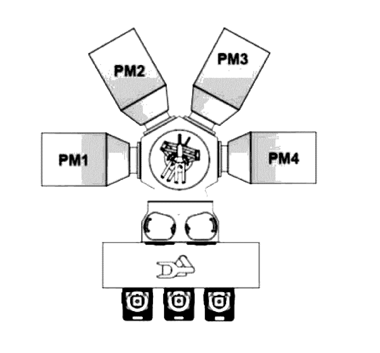
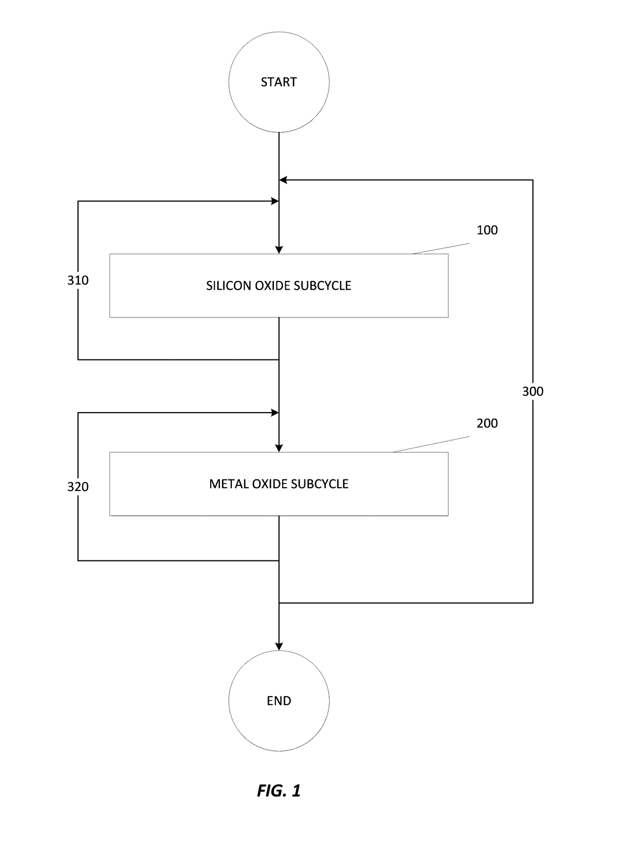
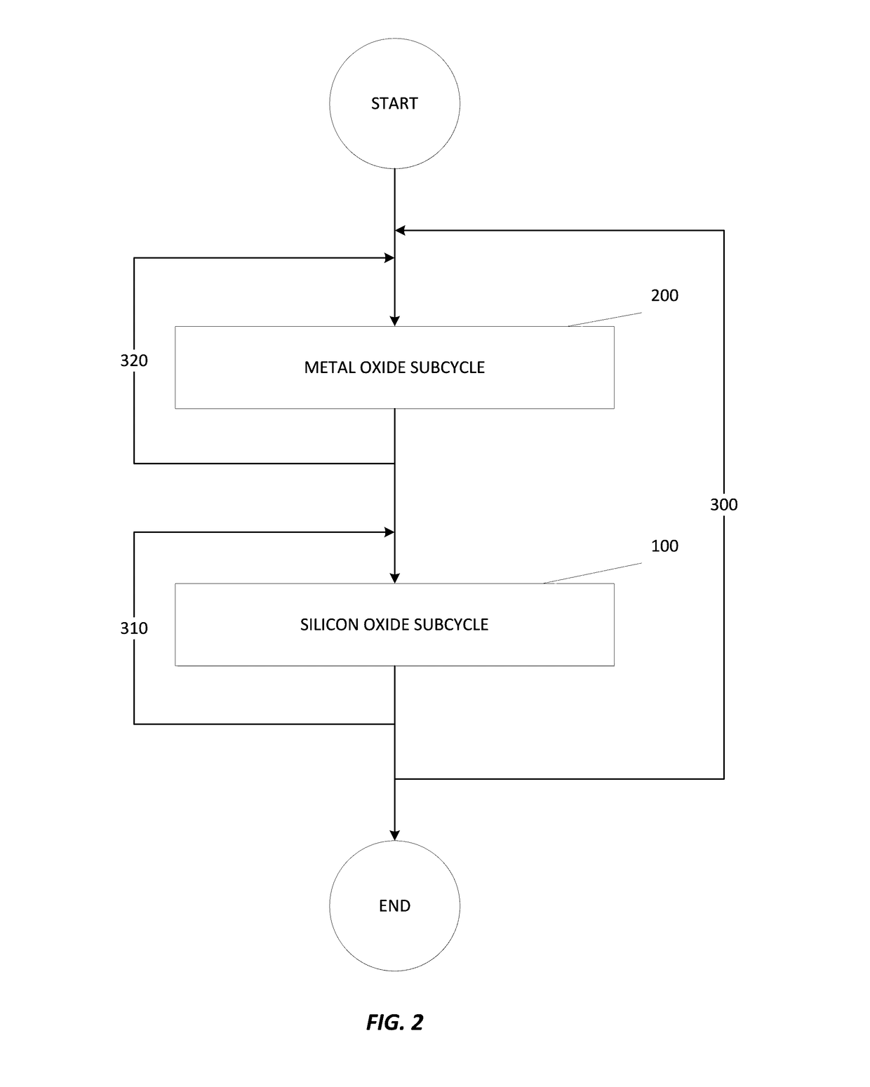
[0022]FIG. 1 illustrates a process in which a transition metal silicate film can be formed on a substrate according to at least one embodiment of the invention. The substrate may be a silicon substrate, a silicon-capped germanium substrate, a Ge substrate, a SiGe substrate, or a III-V semiconductor substrate (such as InGaAs). In order to form a metal silicate film, such as a Lanthanum Silicate (LaSiO) film, a master cycle may comprise two subcycles. One subcycle may be a silicon oxide subcycle 100, while the other subcycle may be a metal oxide subcycle 200. The silicon oxide subcycle 1...


PUM

PropertyMeasurementUnit
temperatureaaaaaaaaaa

Abstract

A method for depositing a thin film onto a substrate is disclosed. In particular, the method forms a transitional metal silicate onto the substrate. The transitional metal silicate may comprise a lanthanum silicate or yttrium silicate, for example. The transitional metal silicate indicates reliability as well as good electrical characteristics for use in a gate dielectric material.

Description

CROSS REFERENCE TO RELATED APPLICATION[0001]The present application claims priority to U.S. Provisional Patent Application No. 62 / 242,804, entitled “Implementing Atomic Layer Deposition Gate Dielectrics for MOSFET Devices” and filed on Oct. 16, 2015, the contents of which are hereby incorporated herein by reference, to the extent such contents do not conflict with the present disclosure.FIELD OF INVENTION[0002]The present disclosure generally relates to processes for manufacturing electronic devices. More particularly, the disclosure relates to forming a Transition Metal Silicate film through atomic layer deposition (ALD).BACKGROUND OF THE DISCLOSURE[0003]Atomic layer deposition (ALD) is a method for depositing a thin film on a substrate through sequential distribution of various precursors. A conventional ALD method can take place in a reaction system comprising a reaction chamber, a substrate holder, a gas flow system, and an exhaust system. Growth of the thin film takes place whe...

Claims


Application Information

Patent Timeline
Patent Type & Authority Applications(United States)
IPC IPC(8): H01L21/02H01L29/78H01L29/20H01L29/51C23C16/455H01L29/16
CPCH01L21/0228H01L21/02274H01L21/02211H01L21/02156H01L29/78H01L29/16H01L29/20H01L29/517C23C16/45544C23C16/0272C23C16/30C23C16/45527H01L21/28194C23C16/401C23C16/45529H01L21/205H01L21/28202H01L21/02208H01L21/02142H01L21/02046H01L21/324
Inventor TANG, FUJIANG, XIAOQIANGXIE, QIGIVENS, MICHAEL EUGENEMAES, JAN WILLEMCHEN, JERRY
Owner ASM IP HLDG BV
Why Eureka
Try Eureka