Methods for forming a semiconductor device and related semiconductor device structures

a technology of semiconductor devices and semiconductor devices, applied in the direction of semiconductor devices, electrical equipment, transistors, etc., can solve the problems of polysilicon not being ideal gate electrode materials for advanced node applications, polysilicon not showing an ideal effective work function (ewf) for both nmos and pmos devices, and depleting of the surface region of carriers

Active Publication Date: 2018-05-03
ASM IP HLDG BV
View PDF12 Cites 305 Cited by
  • Summary
  • Abstract
  • Description
  • Claims
  • Application Information

AI Technical Summary

Benefits of technology

[0004]This summary is provided to introduce a selection of concepts in a simplified form. These concepts are described in further detail in the detailed description of example embodiments of the disc

Problems solved by technology

However, doped polysilicon may not be an ideal gate electrode material for advanced node applications.
For example, although doped polysilicon is conductive, there may still be a surface region which can be depleted of carriers under bias conditions.
As a further example,

Method used


Image

  • Methods for forming a semiconductor device and related semiconductor device structures
  • Methods for forming a semiconductor device and related semiconductor device structures
  • Methods for forming a semiconductor device and related semiconductor device structures

Examples


Embodiment Construction

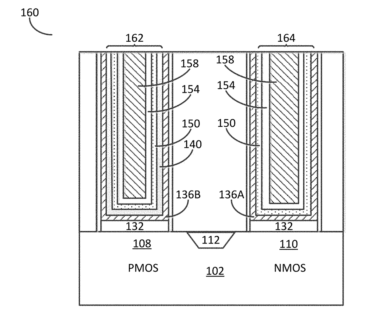
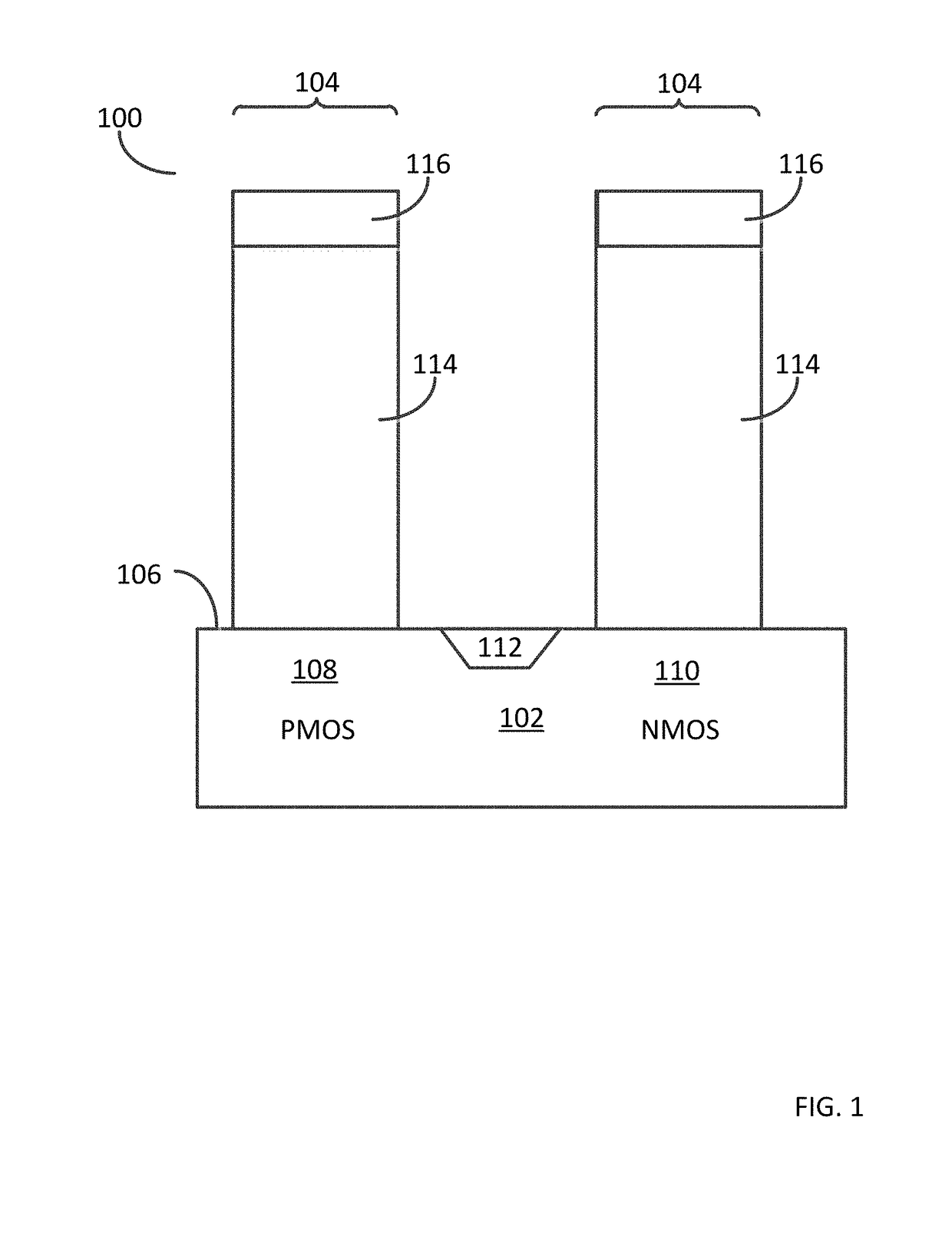
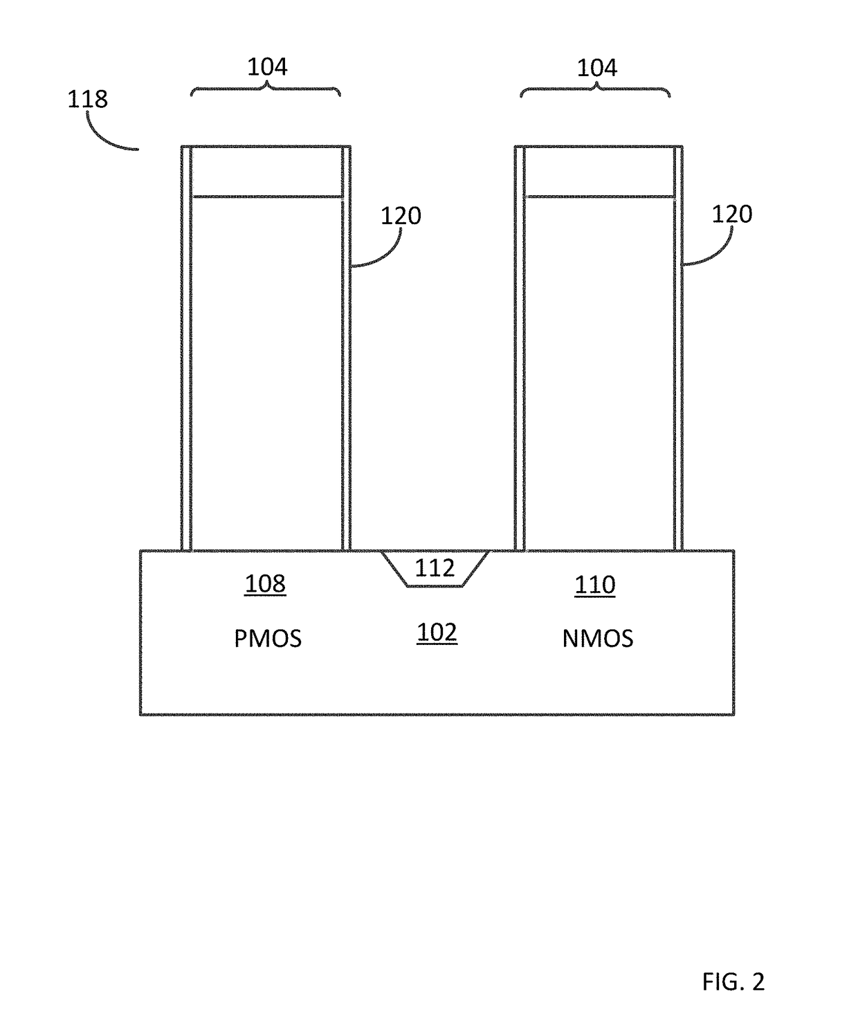
[0011]The illustrations presented herein are not meant to be actual view of any particular material, structure, or device, but are merely idealized representations that are used to describe embodiments of the disclosure.

[0012]As used herein, the term “atomic layer deposition” (ALD) may refer to a vapor deposition process in which deposition cycles, in some instances a plurality of consecutive deposition cycles, are conducted in a process chamber. Typically, during each cycle the precursor is chemisorbed to a deposition surface (e.g., a substrate surface or a previously deposited underlying surface such as material from a previous ALD cycle), forming a monolayer or sub-monolayer that does not readily react with additional precursor (i.e., a self-limiting reaction). Thereafter, if necessary, a reactant (e.g., another precursor or reaction gas) may subsequently be introduced into the process chamber for use in converting the chemisorbed precursor to the desired material on the depositi...


PUM


Abstract

Methods for forming a semiconductor device and related semiconductor device structures are provided. In some embodiments, methods may include forming an NMOS gate dielectric and a PMOS gate dielectric over a substrate and forming a first work function metal over the NMOS gate dielectric and over the PMOS gate dielectric. In some embodiments, methods may also include, removing the first work function metal over the NMOS gate dielectric and forming a second work function metal over the NMOS gate dielectric and over the PMOS gate dielectric. In some embodiments, related semiconductor device structures may include an NMOS gate dielectric and a PMOS gate dielectric disposed over a semiconductor substrate. A PMOS gate electrode may be disposed over the PMOS gate dielectric and the PMOS gate electrode may include a first work function metal disposed over the PMOS gate dielectric and a second work function metal disposed over the first work function metal. A NMOS gate electrode may be disposed over the NMOS gate dielectric and the NMOS gate electrode may include the second work function metal.

Description

BACKGROUNDField of the Invention[0001]The present disclosure relates generally to methods for forming semiconductor devices and particular to forming CMOS semiconductor devices and related semiconductor device structures.Description of the Related Art[0002]Metal-oxide-semiconductor (MOS) technology has conventionally utilized n-type and p-type doped polysilicon as the gate electrode material. However, doped polysilicon may not be an ideal gate electrode material for advanced node applications. For example, although doped polysilicon is conductive, there may still be a surface region which can be depleted of carriers under bias conditions. This region may appear as an extra gate insulator thickness, commonly referred to as gate depletion, and may contribute to the equivalent oxide thickness. While the gate depletion region may be thin, on the order of a few angstroms (Å), it may become significant as the gate oxide thicknesses are reduced in advance node applications. As a further ex...

Claims


Application Information

Patent Timeline
IPC IPC(8): H01L21/8238H01L29/49H01L21/3213H01L21/285H01L27/092H01L21/28H01L29/66
CPCH01L21/823842H01L21/823857H01L29/4966H01L21/32133H01L21/28556H01L27/092H01L21/28088H01L29/66545H01L21/823821H01L27/0924H01L29/6656H01L21/0217H01L21/0228H01L29/517H01L29/42364H01L29/78H01L21/8238H01L21/3213
Inventor XIE, QIGIVENS, MICHAEL EUGENRAISANEN, PETRIMAES, JAN WILLEM
Owner ASM IP HLDG BV
Why Eureka
Try Eureka