LCD device and its display method

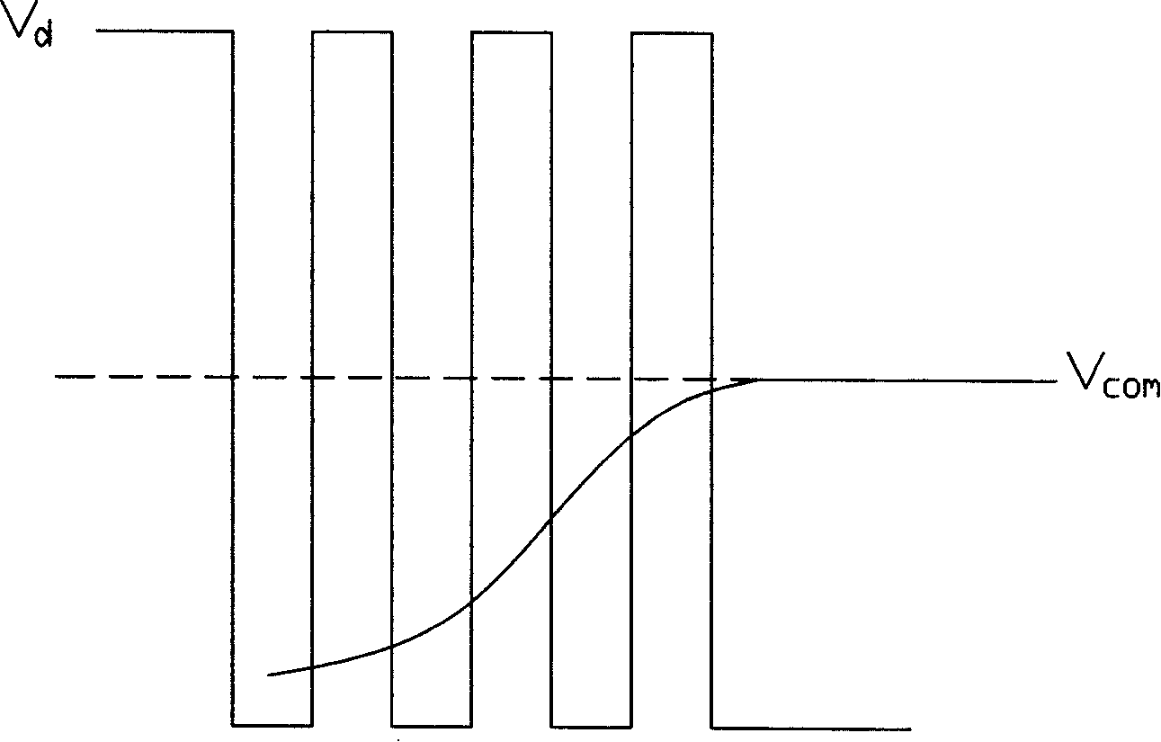
A technology of a liquid crystal display device and a display method, which is applied in static indicators, nonlinear optics, optics, etc., and can solve the problems of liquid crystal capacitors 3 with different light transmittance, charges that cannot be quickly discharged, and voltage differences that are different, and achieve improvement. Shutdown afterimage phenomenon, avoid the effect of boot flickering

Active Publication Date: 2008-07-02
INNOCOM TECH SHENZHEN +1
View PDF0 Cites 44 Cited by
  • Summary
  • Abstract
  • Description
  • Claims
  • Application Information

AI Technical Summary

Problems solved by technology

Usually, when the liquid crystal display device is turned on to display images, the grayscale voltage Vd is generated before the common voltage Vcom, and when the grayscale voltage Vd is transmitted to the pixel electrode 31, the common voltage Vcom of the common electrode 32 still rises in a curve and does not reach a stable value. During the display period of the previous frames, the voltage difference between the common voltage Vcom and the pixel voltage Vd is different, so that the light transmittance of the liquid crystal capacitor 3 is different, so that the liquid crystal display device has a flicker phenomenon
[0006] In addition, the public voltage Vcom is gradually reduced to 0V at the moment of shutdown, and the charge inside the liquid crystal capacitor 3 cannot be quickly discharged, so that there is still a voltage difference between the two ends of the liquid crystal capacitor 3, that is, the electric field driving the deflection of the liquid crystal molecules still exists, and the liquid crystal molecules still have a certain Light transmittance, so the liquid crystal display device shows residual image under external light

Method used


Image

  • LCD device and its display method
  • LCD device and its display method
  • LCD device and its display method

Examples


Embodiment Construction

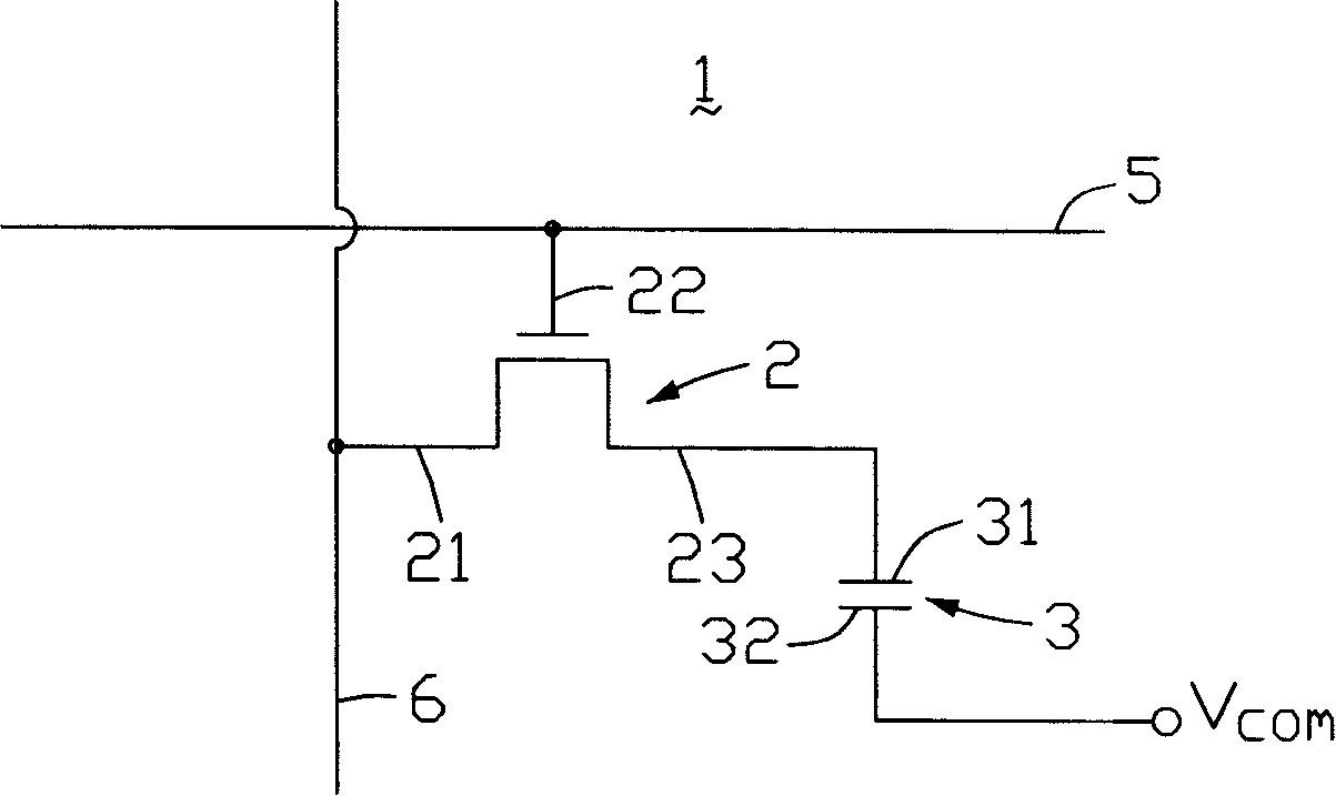
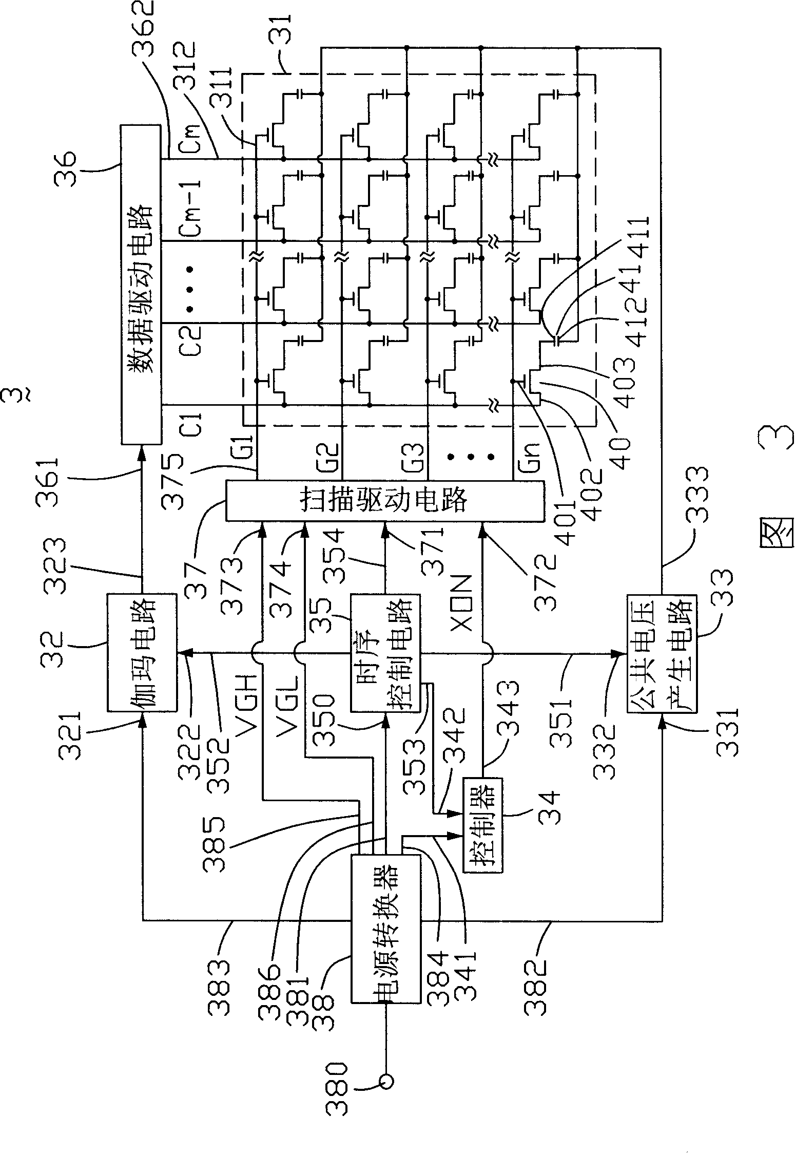
[0018] Please refer to FIG. 3 , which is a schematic diagram of a liquid crystal display device of the present invention. The liquid crystal display device 3 includes a power supply (not shown), a liquid crystal display panel 31, a gamma circuit 32, a common voltage generating circuit 33, a controller 34, a timing control circuit 35, a data drive circuit 36, A scan driving circuit 37 and a power converter 38 .

[0019] The liquid crystal display panel 31 includes a plurality of scanning lines 311 arranged parallel to each other, a plurality of data lines 312 arranged in parallel and vertically insulating and intersecting with the scanning lines 311, a plurality of pixel electrodes 411, and a plurality of data lines 312 located between the scanning lines 311 and the scanning lines 311. The thin film transistor 40 at the intersection of the data lines 312 , a plurality of common electrodes 412 disposed opposite to the pixel electrodes 411 , and a liquid crystal layer (not shown)...


PUM


Abstract

The invention provides a liquid crystal display device which consists of a liquid crystal panel, a sequential control circuit, a common voltage generation circuit, a gamma circuit and a scan driving circuit, wherein, the liquid crystal panel comprises a plurality of thin film transistors, the scan driving circuit is used to control the conduction and closing of the thin film transistors; the sequential control circuit is used to generate a common circuit sequence signal and a gray-stage voltage sequence signal, the two sequence signals control the common voltage generation circuit and the gamma circuit respectively in order that the common voltage generated by the common voltage generation circuit can be transmitted to the liquid crystal panel and to become steady before the gray-staged voltage generated by the gamma circuit is transmitted to the liquid crystal panel when opening the liquid crystal display device, and that the gray-staged voltage and the common voltage reduce to 0V at the same time when a plurality of the thin film transistors are all conducted when closing the liquid crystal display device.

Description

technical field [0001] The invention relates to a liquid crystal display device and a display method thereof. Background technique [0002] Liquid crystal display devices have the advantages of no radiation, thinness, and power saving, and gradually replace traditional CRT (Cathode Ray Tube, CRT) displays. At present, liquid crystal displays have been widely used in various high-quality digital televisions, notebook computers, digital cameras and other electronic products. [0003] see figure 1 , is a schematic circuit diagram of a pixel unit of a prior art liquid crystal display device. The pixel unit 1 includes a scanning line 5, a data line 6, a thin film transistor 2, a pixel electrode 31, a common electrode 32 and a liquid crystal layer (not shown) sandwiched between the two electrodes 31, 32 . The gate 22 of the TFT 2 is electrically connected to the scan line 5 , the source 21 is electrically connected to the data line 6 , and the drain 23 is electrically connecte...

Claims


Application Information

Patent Timeline
Patent Type & Authority Applications(China)
IPC IPC(8): G02F1/133G09G3/36G02F1/1362
Inventor 童建凡黄顺明冯沙
Owner INNOCOM TECH SHENZHEN
Why Eureka
Try Eureka