Array substrate and display panel

A technology of array substrate and color filter substrate, which is applied in the field of display to improve the display effect and improve the effect of after-image after shutdown

Active Publication Date: 2022-03-01
MIANYANG HKC OPTOELECTRONICS TECH CO LTD +1
View PDF6 Cites 0 Cited by
  • Summary
  • Abstract
  • Description
  • Claims
  • Application Information

AI Technical Summary

Problems solved by technology

[0004] The purpose of this application is to provide an array substrate and a display panel, aiming to solve the technical problem of how to reduce the residual charge of the pixel electrodes in the display panel

Method used


Image

  • Array substrate and display panel
  • Array substrate and display panel
  • Array substrate and display panel

Examples


no. 1 example

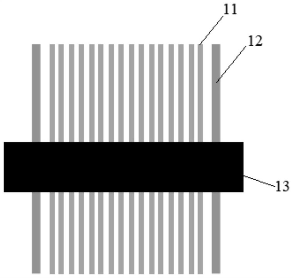
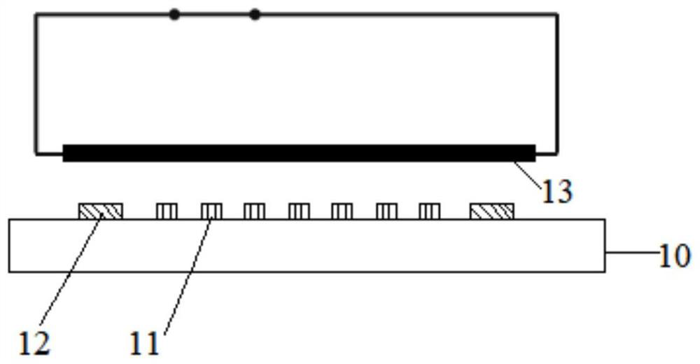
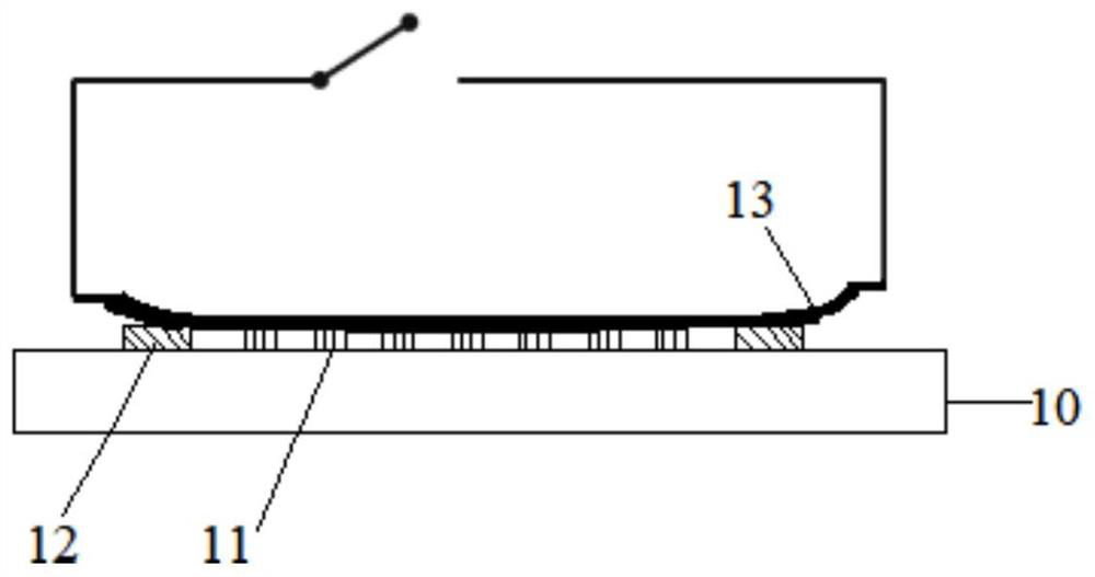
[0038] An array substrate, such as Figure 1-3 As shown, the array substrate includes a substrate 10 and a first lead 11 and a second lead 12 arranged in a non-display area on the substrate 10, the first lead 11 is electrically connected to the pixel electrode, and the second lead 12 is electrically connected to the common electrode or For the ground electrode, the array substrate also includes an electric actuation element 13, and the electric actuation element 13 includes at least one conductive layer; wherein, after the electric actuation element 13 changes from the power-on state to the power-off state, the electric actuation element The conductive layer of the device 13 is deformed and contacts at least part of the first lead 11 and at least part of the second lead 12 .

[0039]The array substrate of this embodiment is provided with a unique electric actuation component 13, which has the effect of electric actuation deformation. When the electric actuation component 13 ch...

no. 2 example

[0046] An array substrate, such as figure 1 , 4 As shown in -5, the array substrate includes a substrate 10 and a first lead 11 and a second lead 12 arranged in a non-display area on the substrate 10, the first lead 11 is electrically connected to the pixel electrode, and the second lead 12 is electrically connected to the common electrode or ground electrode, the array substrate also includes an electric actuation component 13, the electric actuation component 13 includes a laminated first material layer 131 and a second material layer 132, the first material layer 131 is located between the substrate 10 and the second Between the material layers 132, the first material layer 131 is a conductive layer, and the thermal expansion coefficient of the second material layer 132 is greater than that of the first material layer 131; The conductive layer on the lower surface of the actuating component 13 is deformed and contacts at least part of the first lead 11 and at least part of...

no. 3 example

[0055] A display panel includes the array substrate of the embodiment of the present application, a color filter substrate disposed opposite to the array substrate, and a liquid crystal layer located on the array substrate and the color filter substrate. Specifically, the array substrate includes a substrate 10 and a first lead 11 and a second lead 12 arranged in a non-display area on the substrate 10, the first lead 11 is electrically connected to the pixel electrode, and the second lead 12 is electrically connected to the common electrode or For the ground electrode, the array substrate further includes an electric actuation component 13, and the electric actuation component 13 includes at least one conductive layer; wherein, after the electric actuation component 13 changes from the power-on state to the power-off state, the electric actuation component The conductive layer 13 is deformed and contacts at least part of the first lead 11 and at least part of the second lead 12...


PUM

PropertyMeasurementUnit
Thermal expansion coefficientaaaaaaaaaa
Thicknessaaaaaaaaaa

Abstract

The invention relates to the technical field of display, in particular to an array substrate and a display panel. The array substrate comprises a substrate, a first lead and a second lead, the first lead and the second lead are arranged in a non-display area on the substrate, the first lead is electrically connected with the pixel electrode, the second lead is electrically connected with the common electrode or the ground electrode, the array substrate further comprises an electric actuating component, and the electric actuating component comprises at least one conducting layer; and after the electric actuating component is changed from a power-on state to a power-off state, a conductive layer of the electric actuating component is deformed and is in contact with at least part of the first lead and at least part of the second lead. After the conducting layer of the electric actuating component is in contact with the first lead and the second lead, the pixel electrode and the common electrode or the ground electrode can be in short circuit, so that residual charges left on the pixel electrode due to shutdown can be quickly released, the shutdown ghost phenomenon of the display panel can be improved, and the display effect is improved.

Description

technical field [0001] The present application belongs to the field of display technology, and in particular relates to an array substrate and a display panel. Background technique [0002] Generally, a display panel in a liquid crystal display includes an array substrate (Thin Film TransistorArray, TFT), a color filter substrate (Color Filter, CF) and a layer of liquid crystal molecules (Liquid Crystal, LC) sandwiched between the two substrates. In the array substrate, lead wires are also arranged in the non-display area to electrically connect the pixel array and the driving chip. [0003] During the normal operation of the liquid crystal display panel, a certain amount of charge will accumulate on the pixel electrode in the liquid crystal display panel. When it is turned off, because the charge on the pixel electrode cannot be quickly eliminated, there is a certain voltage difference between the pixel electrode and the common electrode. As a result, the display screen wi...

Claims


Application Information

Patent Timeline
IPC IPC(8): G02F1/1362G02F1/1345H01L27/12
CPCG02F1/136204G02F1/13452H01L27/12G02F1/133397G02F1/136222G02F1/136286H01L27/1222G02F1/136272G02F1/1345G02F1/136218
Inventor 唐榕康报虹
Owner MIANYANG HKC OPTOELECTRONICS TECH CO LTD
Why Eureka
Try Eureka