Check patentability & draft patents in minutes with Patsnap Eureka AI!

Nand flash memory device with 3-dimensionally arranged memory cell transistors

A flash memory device, device technology, applied in the direction of electrical solid state devices, semiconductor devices, semiconductor/solid state device components, etc., can solve the problems of complex manufacturing of NAND flash memory devices, reduction of integration degree of NAND flash memory devices, etc.

Inactive Publication Date: 2008-09-03
SAMSUNG ELECTRONICS CO LTD
View PDF0 Cites 17 Cited by
  • Summary
  • Abstract
  • Description
  • Claims
  • Application Information

AI Technical Summary

Problems solved by technology

The need for separate well plugs reduces the integration level of NAND-type flash memory devices and makes the fabrication of NAND-type flash memory devices more complex

Method used


Image

  • Nand flash memory device with 3-dimensionally arranged memory cell transistors
  • Nand flash memory device with 3-dimensionally arranged memory cell transistors
  • Nand flash memory device with 3-dimensionally arranged memory cell transistors

Examples


Embodiment Construction

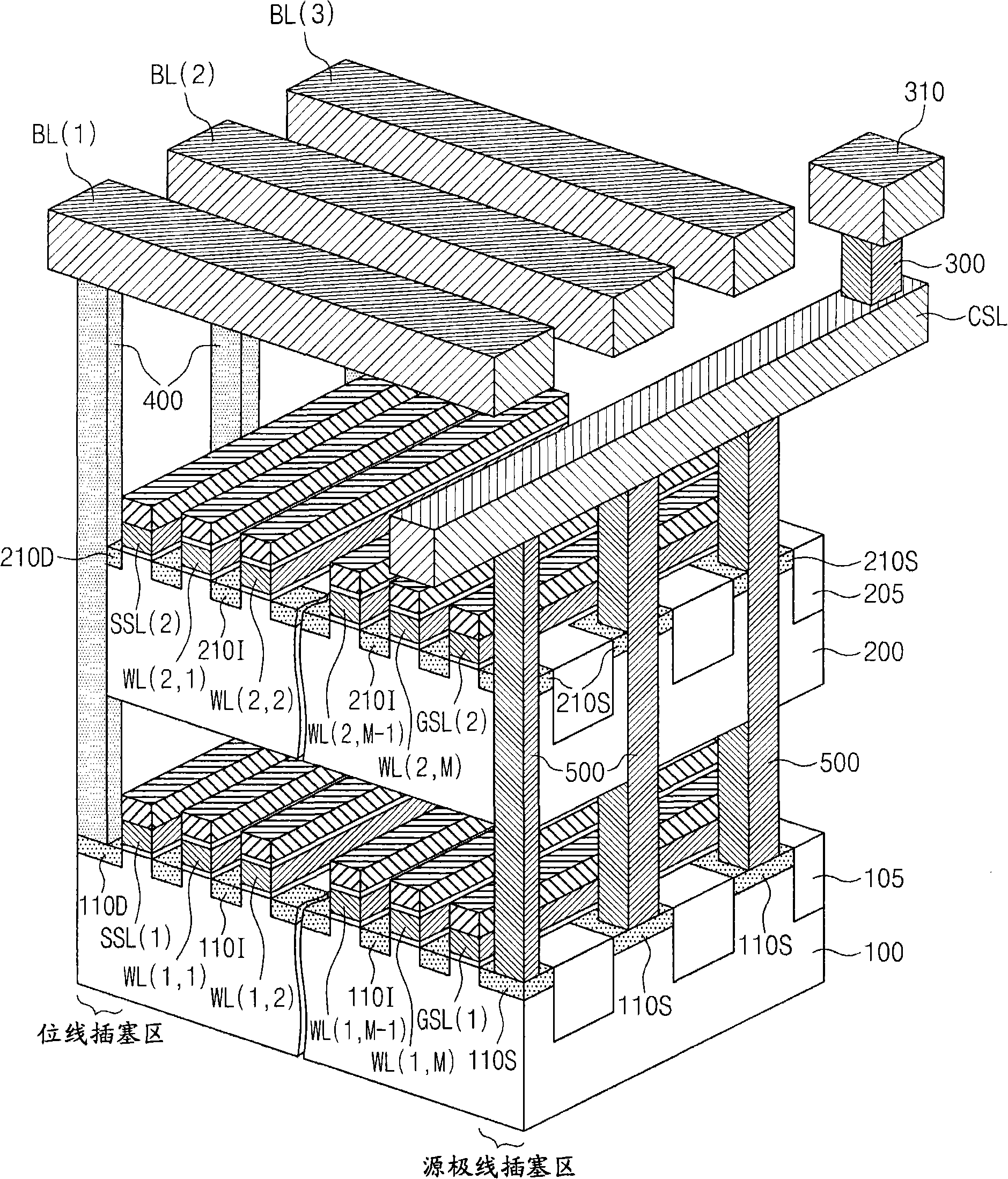
[0034] The present invention will be described more fully hereinafter with reference to the accompanying drawings, in which typical embodiments of the invention are shown. However, this invention may be embodied in different forms and should not be construed as limited to the embodiments set forth herein. Rather, these embodiments are provided so that this disclosure will be thorough and complete, and will fully convey the scope of the invention to those skilled in the art.

[0035]It will be understood that terms such as "first" and "second" may be used herein to describe different regions, layers and / or sections. These terms are used to distinguish one region, layer and / or section from another region, layer and / or section. However, these regions, layers and / or sections should not be limited by these terms. In the drawings, the dimensions of layers and regions may be exaggerated for clarity of illustration. It will also be understood that when a layer or element is referre...


PUM


Abstract

A NAND flash memory device includes a plurality of stacked semiconductor layers, device isolation layer patterns disposed in predetermined regions of each of the plurality of semiconductor layers, the device isolation layers defining active regions, source and drain impurity regions in the active regions, a source line plug structure electrically connecting the source impurity regions, and a bit-line plug structure electrically connecting the drain impurity regions, wherein the source impurity regions are electrically connected to the semiconductor layers.

Description

technical field [0001] The present invention relates to a semiconductor device. More particularly, the present invention relates to a NAND type flash memory device having three-dimensionally arranged memory cell transistors. Background technique [0002] Electronic products such as computers, mobile phones, multimedia players, digital cameras, etc. may contain semiconductor devices such as a memory chip for storing information and a processing chip for controlling information. A semiconductor device may contain electronic components such as transistors, resistors, capacitors, and the like. Electronic components can be integrated on semiconductor substrates, and a high level of integration may be required in order to provide high performance and reasonable prices that meet consumer demands. [0003] In order to achieve a high degree of integration, advanced process technologies such as photolithography processes may be required in the fabrication of semiconductor devices. ...

Claims


Application Information

Patent Timeline
IPC IPC(8): H01L27/115H01L23/522
Inventor 郑载勋金奇南郑舜文张在焄
Owner SAMSUNG ELECTRONICS CO LTD
Features
  • R&D
  • Intellectual Property
  • Life Sciences
  • Materials
  • Tech Scout
  • Unparalleled Data Quality
  • Higher Quality Content
  • 60% Fewer Hallucinations
Learn More