Chip stack package structure
A packaging structure and chip stacking technology, applied in the direction of electrical components, electric solid devices, circuits, etc., can solve the problems of miniaturization and high density of packaging structure, thick chip stacking thickness, high process cost, etc. Low efficiency, solve the effect of low packaging density
- Summary
- Abstract
- Description
- Claims
- Application Information
AI Technical Summary
Problems solved by technology
Method used
Image

Examples
Embodiment Construction
[0095] In order to make the above and other objects, features, advantages and embodiments of the present invention more comprehensible, several chip stack packaging structures are provided as preferred embodiments for further description.
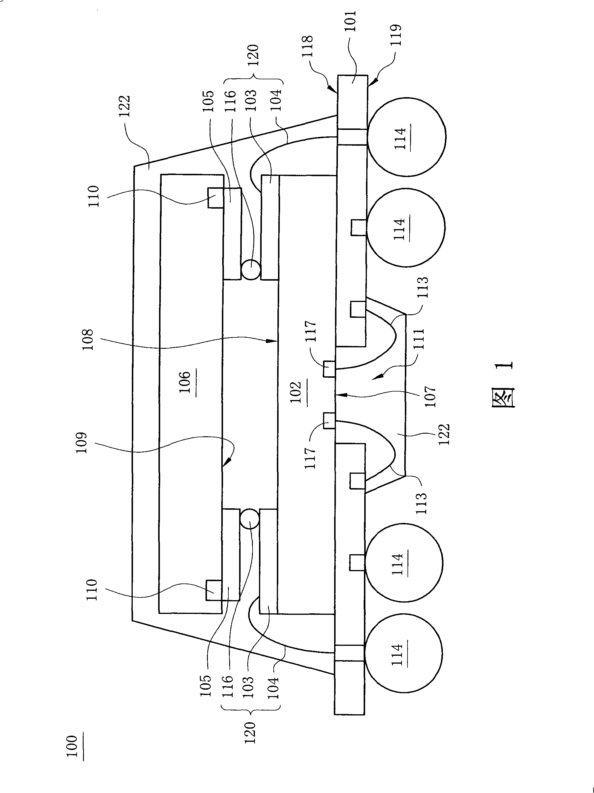
[0096] Please refer to FIG. 1 , which is a schematic cross-sectional view of a chip stack package structure 100 according to a first preferred embodiment of the present invention.
[0097] The chip stack package structure 100 includes: a substrate 101 , a first chip 102 , a patterned circuit layer 105 , a second chip 106 , a conductive component 120 , a sealing resin 122 and a plurality of external connection terminals 111 .
[0098] The substrate 101 has a first surface 118 and a second surface 119 opposite to the first surface 118 . In a preferred embodiment of the present invention, the substrate 101 is constituted by a lead frame, a printed circuit board or a die carrier. In this embodiment, the base material 101 is a printed circuit b...
PUM
 Abstract
Description
Claims
Application Information
 - R&D
- Intellectual Property
- Life Sciences
- Materials
- Tech Scout
- Unparalleled Data Quality
- Higher Quality Content
- 60% Fewer Hallucinations
Browse by: Latest US Patents, China's latest patents, Technical Efficacy Thesaurus, Application Domain, Technology Topic, Popular Technical Reports.
© 2025 PatSnap. All rights reserved.Legal|Privacy policy|Modern Slavery Act Transparency Statement|Sitemap|About US| Contact US: help@patsnap.com