A microwave chip supporting structure

A microwave chip and support structure technology, applied in the direction of electrical components, printed circuits, electrical solid devices, etc., can solve problems such as interference chips and/or bonding wires

Inactive Publication Date: 2009-05-13
TELEFON AB LM ERICSSON (PUBL)
View PDF6 Cites 2 Cited by
  • Summary
  • Abstract
  • Description
  • Claims
  • Application Information

AI Technical Summary

Problems solved by technology

[0013] -Adhesive or solder must be applied to the conductors on ...

Method used


Image

  • A microwave chip supporting structure
  • A microwave chip supporting structure
  • A microwave chip supporting structure

Examples


Embodiment Construction

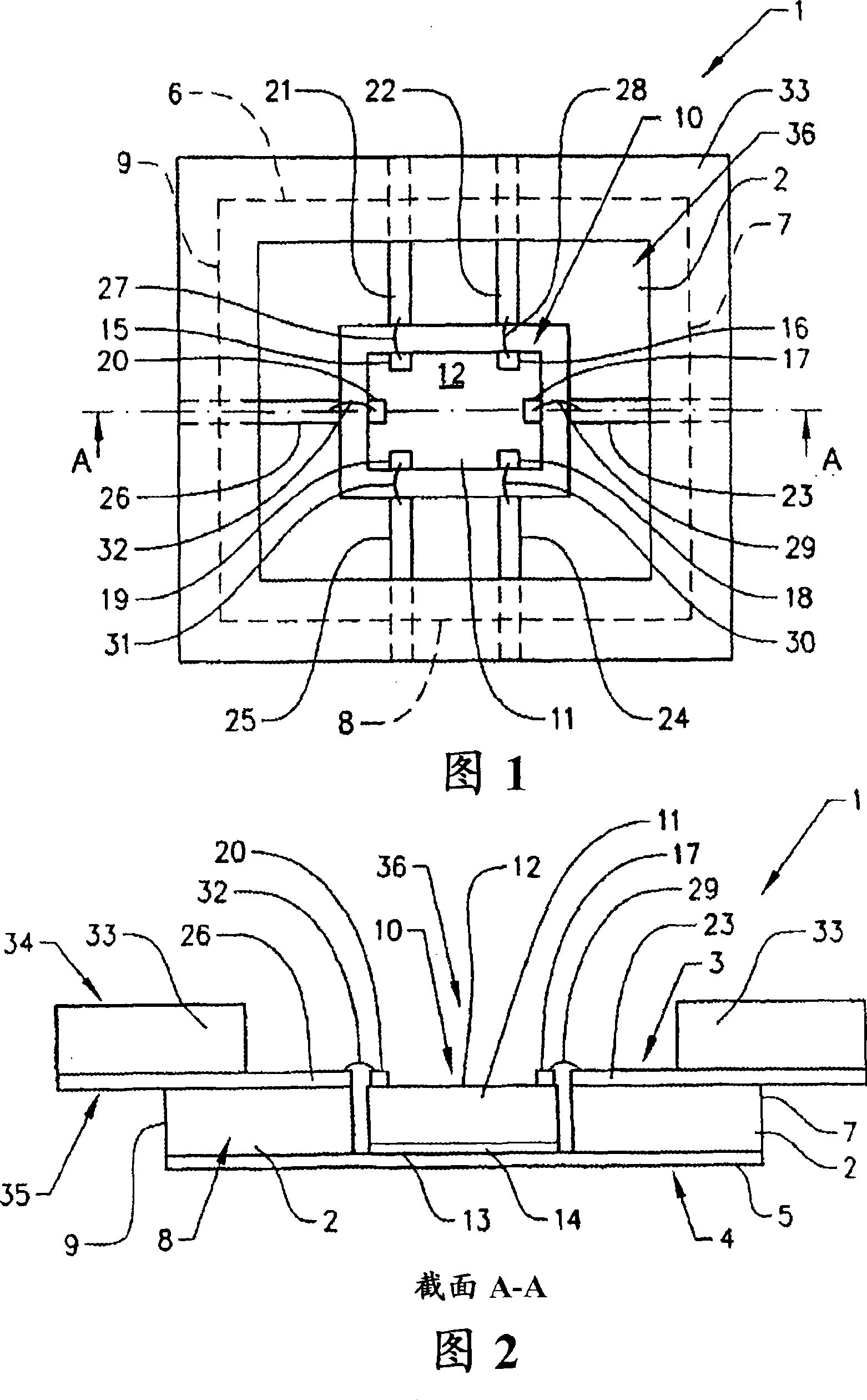
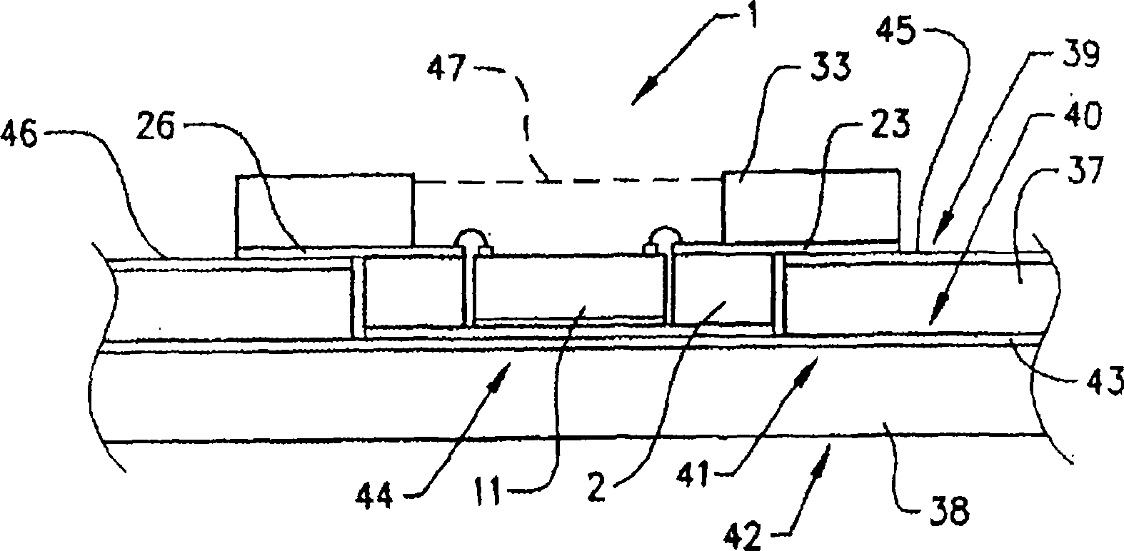
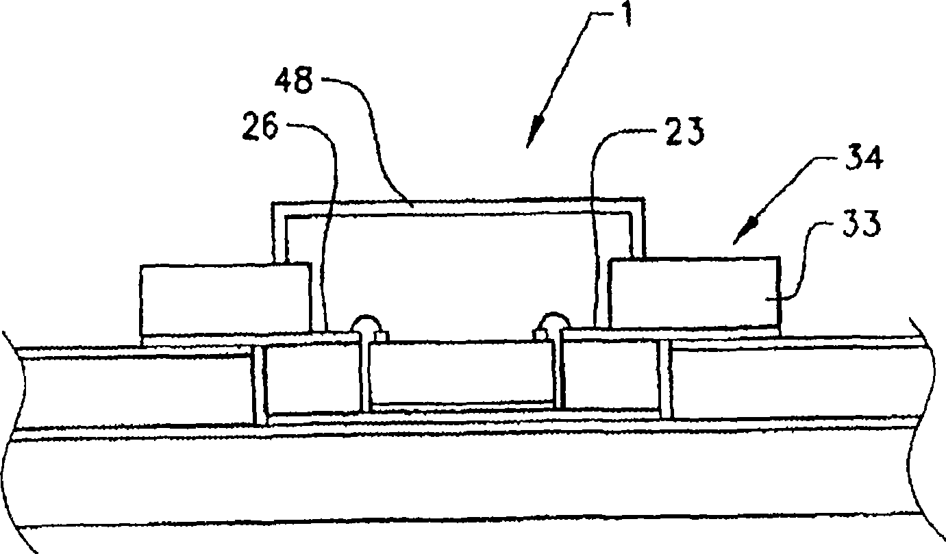
[0034] In FIGS. 1 and 2 a first embodiment is shown showing a microwave chip support structure 1 . The support structure 1 comprises a first microwave laminate layer 2 , for example based on PTFE, with a first side 3 and a second side 4 , wherein a copper ground plane 5 is fixed to the second side 4 . Delimited by a first edge 6, a second edge 7, a third edge 8 and a fourth edge 9, the first laminate layer 2 is substantially rectangular. A first recess 10 is formed in the first laminate layer 2, wherein the first recess 10 is formed in such a way that a part of the copper ground plane 5 forms an accessible surface for the microwave chip 11 by means such as soldering or gluing Fix this part next to the copper ground plane 5. The chip 11 generally consists of a circuit with etched components on a silicon substrate. The chip 11 has a top side 12 and a bottom side 13, the bottom side 13 facing the ground plane. Thereby, the ground of the chip can be directly connected to the gr...


PUM


Abstract

The present invention relates to a microwave chip supporting structure (1, 1', 1'', 1''') comprising a first microwave laminate layer (2, 49), with a first side (3, 50) and a second side (4, 51), and an outer limit (6, 7, 8, 9; 53, 54, 55, 56). At least one conductor (21, 22, 23, 24, 25, 26; 60, 61, 62, 63, 64, 65) is formed on said first side (3, 50), extending towards said outer limit (6, 7, 8, 9; 53, 54, 55, 56). The microwave chip supporting structure (1, 1', 1'', 1''') further comprises a second microwave laminate layer (33, 33'; 57), with a first side (34, 58) and a second side (35, 59), the second side (35, 59) of the second laminate layer (33, 33', 57) being fixed to at least a part of the first side (3, 50) of the first laminate layer (2, 49). The first laminate layer (2, 49) and/or the second laminate layer (33, 33'; 57) comprises at least one recess (10, 36, 66) arranged for receiving a microwave chip (11, 67) intended to be connected to said conductor (21, 22, 23, 24, 25, 26; 60, 61, 62, 63, 64, 65). The second laminate layer (33, 57) extends outside the outer limit (6, 7, 8, 9; 53, 54, 55, 56) of the first laminate layer (2, 49), said conductors (21, 22, 23, 24, 25, 26; 60, 61, 62, 63, 64, 65) continuing on the second side (35, 59) of the second laminate layer (33, 57) without contacting the first laminate layer (2, 49).

Description

technical field [0001] The present invention relates to a microwave chip support structure comprising a first microwave laminate layer having a first side and a second side, the first microwave laminate layer having an outer limit, and wherein at least one conductor is in a first Formed on the side, the conductors extend toward the outer limit of the first laminate layer. Background technique [0002] In microwave technology, it has become technically feasible to integrate circuits into commercial packages for mass production and sale. Previously, a circuit board had to be designed and discrete components mounted on it, wherein a matching procedure was often then necessary in order to debug the circuit. These packaged integrated microwave circuits thus make microwave design easier and more economical than ever before. [0003] A large number of such packages have been developed in recent years. Packages typically include circuitry with etched components on a silicon subst...

Claims


Application Information

Patent Timeline
IPC IPC(8): H01L23/31
CPCH05K1/183H01L23/057H01L24/48H01L2224/32225H01L2924/1517H01L23/66H01L2924/01079H01L23/5385H01L2924/3011H01L2224/48091H01L2224/49175H01L2224/48227H01L2224/73265H05K2201/10727H05K1/0243H01L2924/15153H01L2924/16152H01L24/49H01L23/24H01L2224/45144H01L2924/30107H01L2924/30111H01L2924/00014H01L24/45H01L2924/00H01L2924/00015H01L2224/05599
Inventor P·利冈德
Owner TELEFON AB LM ERICSSON (PUBL)
Why Eureka
Try Eureka