

Flaw detection method and apparatus
A defect detection and defect technology, which is applied in measuring devices, semiconductor/solid-state device testing/measurement, image data processing, etc., can solve problems such as frequency increase, defect detection accuracy, and inability to detect short circuits
- Summary
- Abstract
- Description
- Claims
- Application Information
AI Technical Summary
Problems solved by technology
Method used
Image

Examples
Embodiment Construction
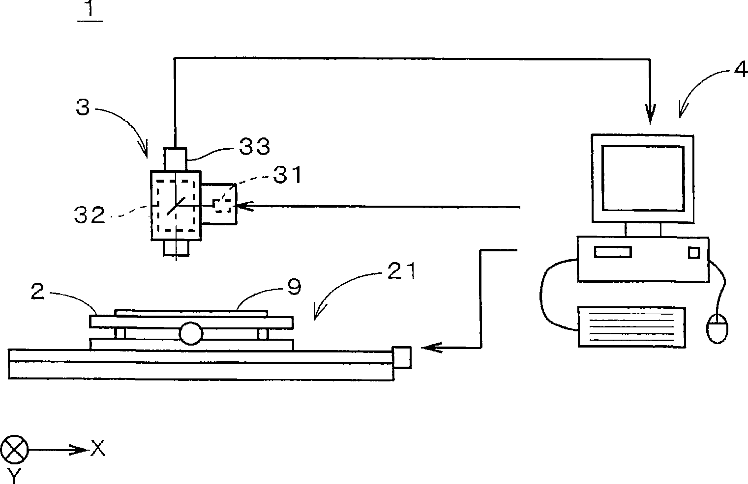
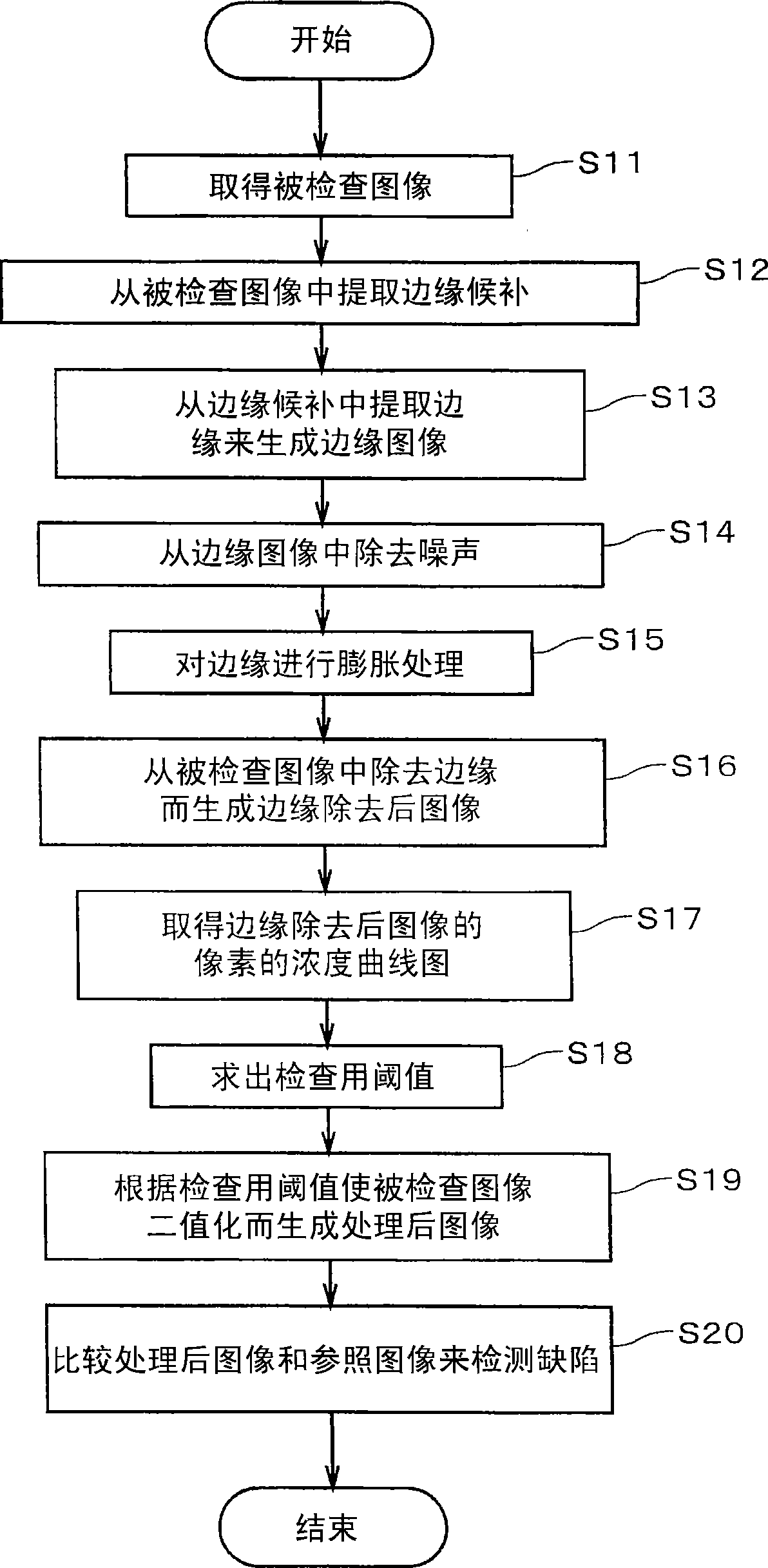
[0034] figure 1 It is a figure which shows the structure of the defect detection apparatus 1 of 1st Embodiment of this invention. The defect detection device 1 is used to detect a defect of a pattern to be detected from a substrate on which a geometric pattern is formed on a main surface of a substrate main body. In this embodiment, defects such as a short circuit (short) of a wiring pattern on a printed wiring board (hereinafter referred to as a "board") are detected by the defect detection device 1 .
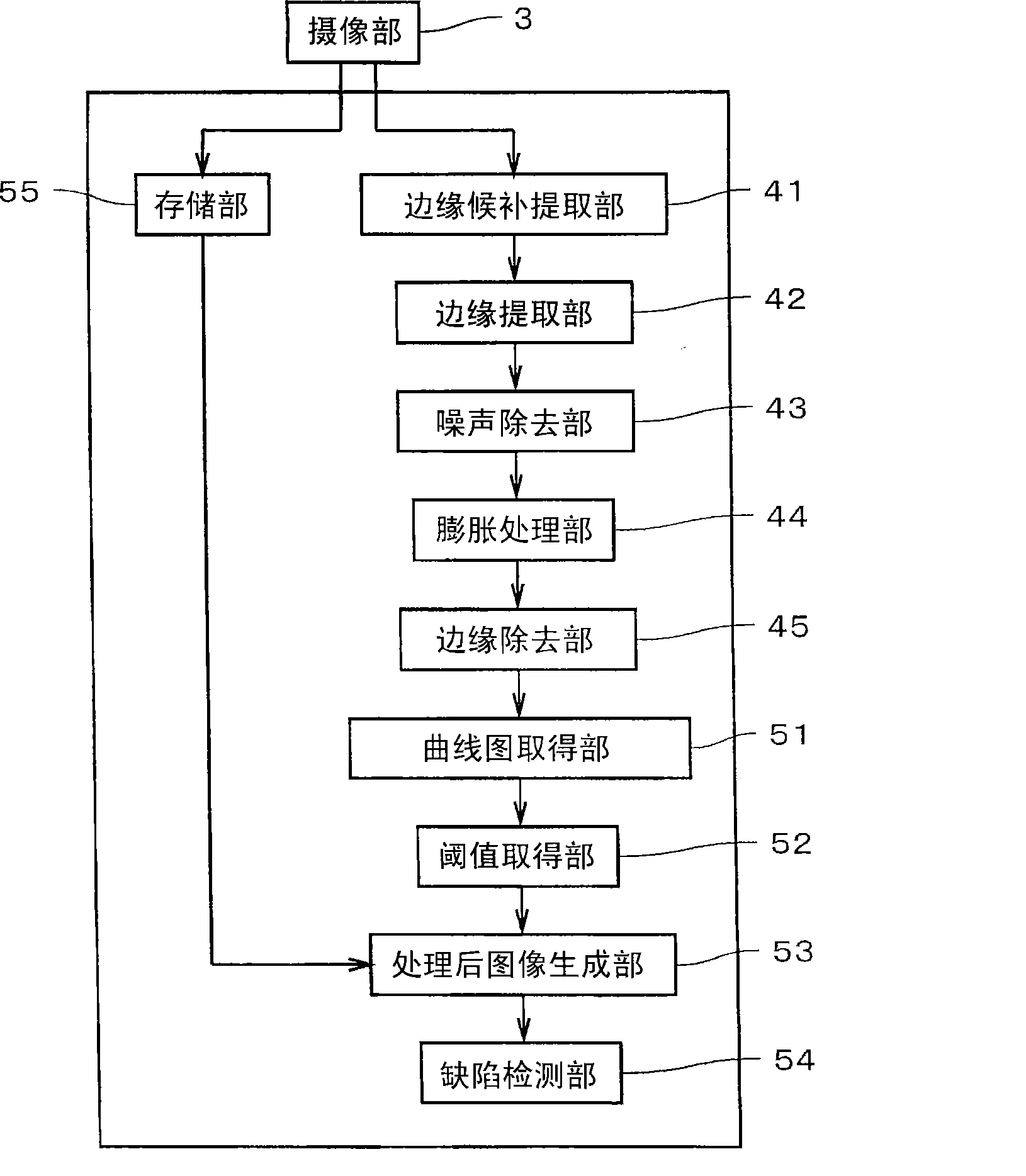
[0035] Defect inspection device 1 has: stage 2, which is used to hold substrate 9; imaging unit 3, which images substrate 9 to obtain multi-gray-scale images of substrate 9; stage drive unit 21, which makes the loading The table 2 moves relative to the imaging unit 3, and the computer 4 is composed of a CPU for performing various arithmetic processing, a memory for storing various information, and the like. And each structure of the defect detection apparatus 1 is controlled...
PUM
 Abstract
Description
Claims
Application Information