Electrophoretic display device and method of manufacturing electrophoretic display device
一种电泳显示、制造方法的技术,应用在图纹面的照相制版工艺、仪器、光学等方向,能够解决消耗电力增大、显示复杂、电泳显示装置可靠性下降等问题
- Summary
- Abstract
- Description
- Claims
- Application Information
AI Technical Summary
Problems solved by technology
Method used
Image

Examples
no. 1 Embodiment approach
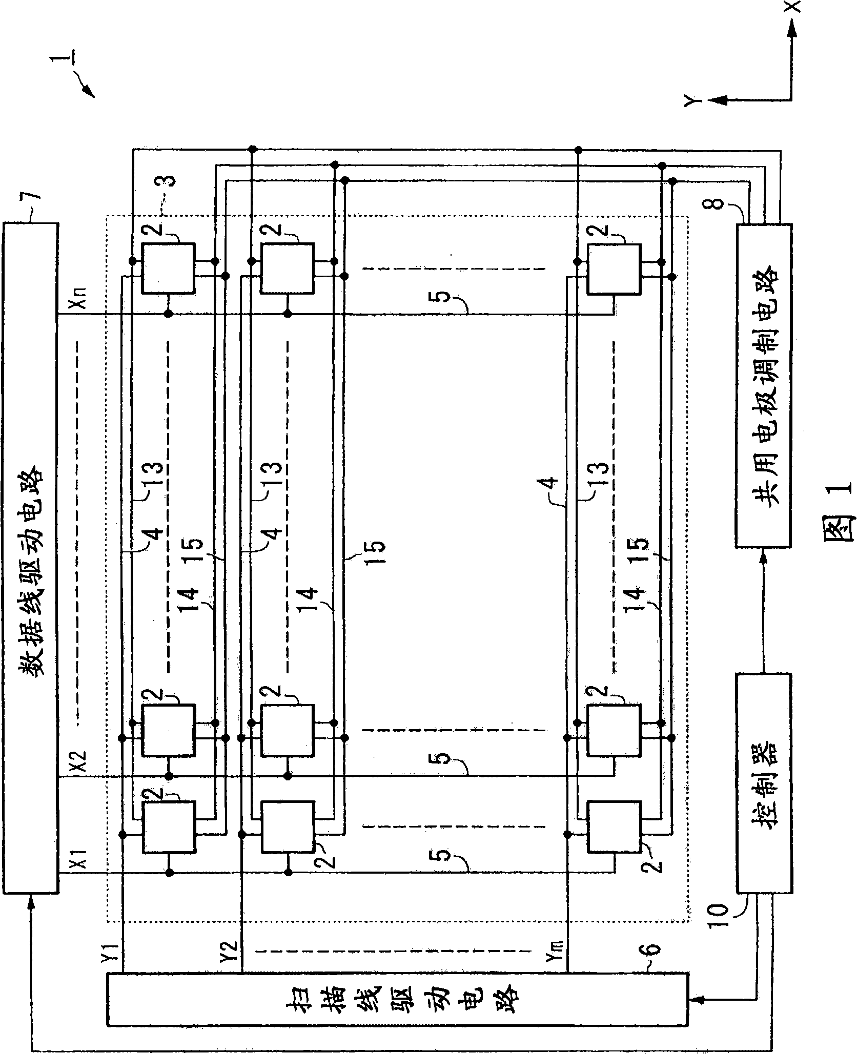
[0056] figure 1 , is a configuration diagram showing the first embodiment of the electrophoretic display device of the present invention, figure 1 Reference numeral 1 is an electrophoretic display device. This electrophoretic display device 1 includes a display unit 3 , a scanning line driving circuit 6 , a data line driving circuit 7 , a common power supply modulation circuit 8 , and a controller 10 .
[0057] In the display unit 3 , M pixels 2 along the Y-axis direction and N pixels 2 along the X-axis direction are formed in a matrix. The scanning line drive circuit 6 is connected to the pixels 2 via a plurality of scanning lines 4 ( Y1 , Y2 , . . . , Ym) extending along the X-axis direction on the display unit 3 . The data line drive circuit 7 is connected to the pixels 2 via a plurality of data lines 5 (X1, X2, . . . , Xn) extending along the Y-axis direction on the display unit 3 . The common power supply modulation circuit 8 is connected to the pixels 2 through the co...
no. 2 Embodiment approach
[0124] Figure 12 , is a diagram showing a second embodiment of the electrophoretic display device of the present invention, and is a cross-sectional view of a main part of the display unit 3 .
[0125] This second embodiment is the same as shown in image 3 The difference from the first embodiment lies in the configuration of the insulating layer 31 . ie, shown in Figure 12 The insulating layer 31 covers only the region between the pixel electrodes 21 and 21, and its upper surface protrudes toward the electrophoretic layer 23 side than the upper surface of the pixel electrode 21. However, it does not need to protrude beyond the upper surface of the pixel electrode 21 as long as the leakage current can be sufficiently suppressed.
[0126] Figure 13 , is a plan view of the display portion 3 showing only the insulating layer 31 and the pixel electrode 21 in the second embodiment. The insulating layer 31 is formed along the region between the pixel electrodes 21 in a grid ...
no. 3 Embodiment approach
[0129] Figure 14 , is a diagram showing a third embodiment of the electrophoretic display device of the present invention, and is a cross-sectional view of a main part of the display unit 3 .
[0130] This third embodiment is the same as shown in image 3 The difference of the first embodiment also lies in the configuration of the insulating layer 31 . ie, shown in Figure 14 The insulating layer 31 is formed only in the central part of the region between the pixel electrodes 21 and 21, and is formed away from the pixel electrode 21. Furthermore, the upper surface of the insulating layer 31 protrudes from the upper surface of the pixel electrode 21 toward the electrophoretic layer 23 side.
[0131] Figure 15 , is a plan view of the display unit 3 showing only the insulating layer 31 and the pixel electrode 21 in the third embodiment. The insulating layer 31 is formed in a grid-like shape in plan view as a whole so as to surround the pixel electrodes 21 in the region bet...
PUM
 Abstract
Description
Claims
Application Information
 - R&D
- Intellectual Property
- Life Sciences
- Materials
- Tech Scout
- Unparalleled Data Quality
- Higher Quality Content
- 60% Fewer Hallucinations
Browse by: Latest US Patents, China's latest patents, Technical Efficacy Thesaurus, Application Domain, Technology Topic, Popular Technical Reports.
© 2025 PatSnap. All rights reserved.Legal|Privacy policy|Modern Slavery Act Transparency Statement|Sitemap|About US| Contact US: help@patsnap.com