Device and method for detecting testing environment of circuit

A testing device and testing environment technology, applied in electronic circuit testing, electromagnetic field characteristics, etc., can solve the problems of general products and methods that do not have suitable structures and methods, and inconvenience.

Active Publication Date: 2009-11-18
KING YUAN ELECTRONICS
View PDF0 Cites 2 Cited by
  • Summary
  • Abstract
  • Description
  • Claims
  • Application Information

AI Technical Summary

Problems solved by technology

[0004] It can be seen that the above-mentioned existing loop test method obviously still has inconvenience and defects in the manufacturing method and use, and needs to be further improved urgently.
In order to solve the above-mentioned problems, the relevant manufacturers have tried their best to find a solution, but no suitable design has been developed for a long time, and there is no suitable structure and method for general products and methods to solve the above-mentioned problems. This is obviously a problem that relevant industry players are eager to solve

Method used


Image

  • Device and method for detecting testing environment of circuit
  • Device and method for detecting testing environment of circuit
  • Device and method for detecting testing environment of circuit

Examples


Embodiment Construction

[0036] In order to further explain the technical means and effects of the present invention to achieve the intended purpose of the invention, the specific implementation of the device and method for detecting the test environment of the circuit according to the present invention will be described below in conjunction with the accompanying drawings and preferred embodiments. , structure, method, step, feature and effect thereof, detailed description is as follows.

[0037] The aforementioned and other technical contents, features and effects of the present invention will be clearly presented in the following detailed description of preferred embodiments with reference to the drawings. For convenience of description, in the following embodiments, the same elements are denoted by the same numbers.

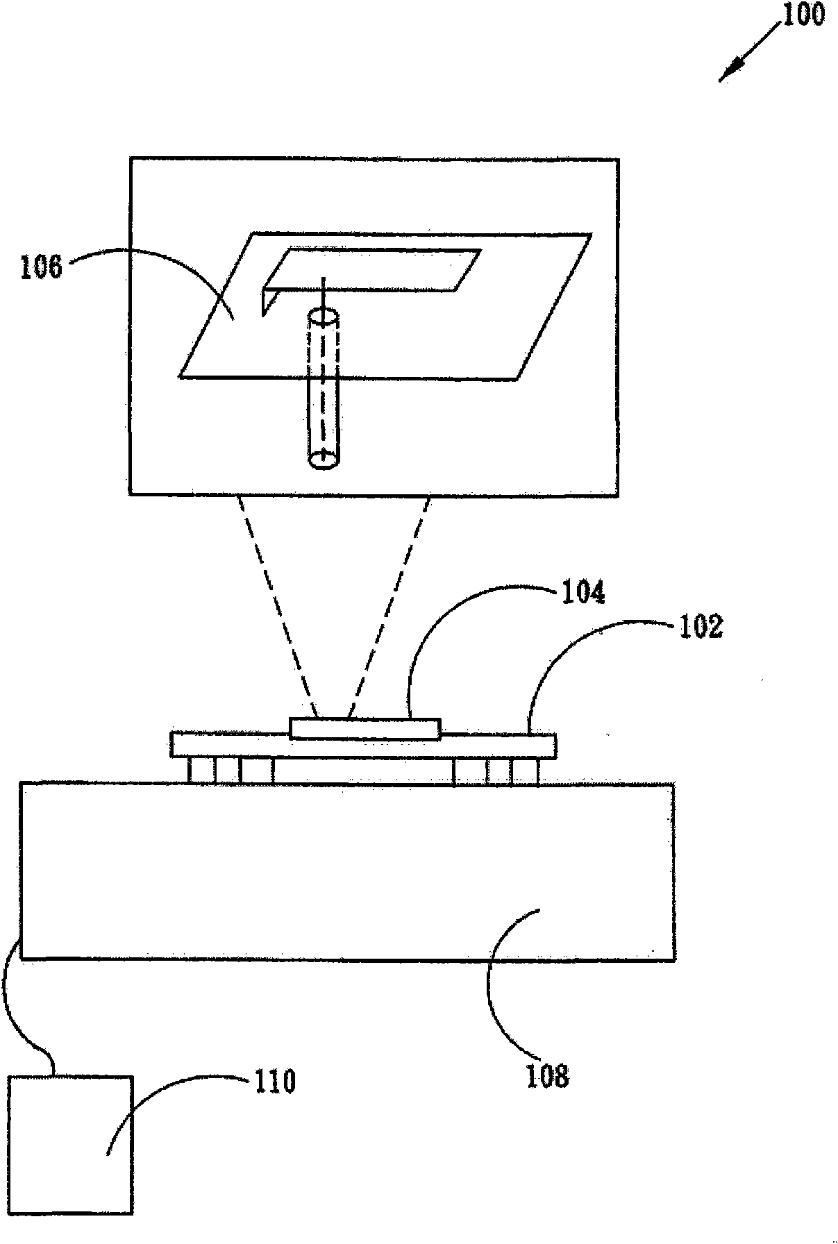
[0038] figure 1 A schematic diagram showing the detection device of the present invention used in the testing environment of integrated circuits. Such as figure 1 As shown, the tes...


PUM


Abstract

The invention relates to a device and a method for detecting testing environment of a circuit. The detecting device mainly comprises a testing support plate, a slot and an antenna, wherein the testing support plate is positioned at the bottom of the detecting device; the slot is arranged on the testing support plate and used for fixing an element to be detected, such as an integrated circuit, and the element to be detected is electrically connected with the testing support plate; and the antenna is arranged on the testing support plate adjacent to the slot and used for receiving wireless signals and monitoring whether the testing environment has excessive foreign signals or not to influence the testing of the circuit.

Description

technical field [0001] The invention relates to a detection device, in particular to a detection device for testing the detection environment of an integrated circuit. Background technique [0002] In the manufacturing process of semiconductors, the manufacturing process of integrated circuits needs to go through a series of tests before they can be sold in the market. In the manufacturing process of radio frequency circuits, the customer will request to do the detection action of the production line environment before the mass production. The code (Pass-bin) will become an invalid code (Fail-bin) or the invalid code (Fail-bin) will become a valid code (Pass-bin), resulting in a test error. Therefore, usually before the mass production of the production line, there will be restrictions on the use of wireless communication equipment or other conditions that will affect the testing of high-frequency components. However, the general loop test only provides regional protection...

Claims


Application Information

Patent Timeline
Patent Type & Authority Applications(China)
IPC IPC(8): G01R29/08G01R31/28
Inventor 柯宣仲谢辰阳
Owner KING YUAN ELECTRONICS
Why Eureka
Try Eureka