Over-erasing processing method and processing system of nonvolatile memory

A technology of non-volatile memory and processing method, which is applied in the field of semiconductor memory, can solve the problems of reducing the overall efficiency of testing and taking a long time, and achieve the effects of saving processing time, improving efficiency, and improving accuracy

Active Publication Date: 2012-11-28
GIGADEVICE SEMICON (BEIJING) INC
View PDF7 Cites 21 Cited by
  • Summary
  • Abstract
  • Description
  • Claims
  • Application Information

AI Technical Summary

Problems solved by technology

However, the secondary programming only operates on some memory cells. When voltage needs to be applied, it needs to be carried out one

Method used


Image

  • Over-erasing processing method and processing system of nonvolatile memory
  • Over-erasing processing method and processing system of nonvolatile memory
  • Over-erasing processing method and processing system of nonvolatile memory

Examples


Embodiment 1

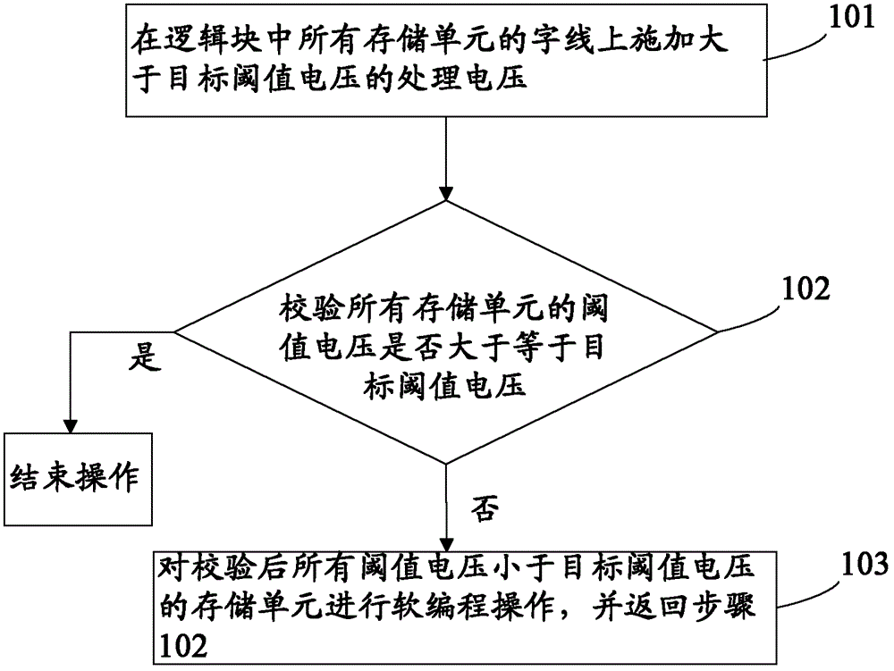
[0045] refer to figure 1 , showing a first embodiment of a non-volatile memory over-erasing processing method of the present invention, including the following steps:

[0046] Step 101 , applying a processing voltage greater than a target threshold voltage to word lines (wordline, WL) of all memory cells in a logic block.

[0047] By applying a processing voltage greater than the target threshold voltage on the word lines of all memory cells in the logic block, the threshold voltage of the memory cells can be increased, and the operation can shorten the overall over-erase processing time of a logic block, thereby improving over-erase removal efficiency.

[0048] Wherein, the magnitude of the processing voltage is determined by the sum of the target threshold voltage and the overdrive voltage. The target threshold voltage is the minimum value of the threshold voltage range that satisfies the normal erasing state in a process flow. For example, the threshold voltage of "less ...


PUM


Abstract

The invention provides an over-erasing processing method of a nonvolatile memory. The method comprises the following steps: applying a processing voltage higher than the target threshold voltage to the word lines of all memory units in a logic block; verifying whether the threshold voltage of each memory unit is higher than or equal to the target threshold voltage; if so, ending the operation; otherwise, going to the next step; and performing soft programming operation on all memory units of which the threshold voltage is lower than the target threshold voltage after the verification, and returning to the previous step. The invention also provides an over-erasing processing system of a nonvolatile memory, which is used for realizing the method. The over-erasing processing method and processing system of a nonvolatile memory provided by the invention can quickly recover all memory units to the normal erasing state, thereby saving the over-erasing processing time and improving the test efficiency.

Description

technical field [0001] The invention relates to the technical field of semiconductor memory, in particular to an over-erasing processing method and processing system of a non-volatile memory. Background technique [0002] In order to verify the correctness of memory products, a series of testing procedures will be carried out before the products leave the factory. These storage products may include non-volatile memory products (for example, flash memory Flash, or electrically erasable programmable read-only memory EEPROM, etc.), and may also include one-time programmable OTP memory. The general test process can include product pin (pin) short circuit / open circuit test, logic function test, electrical erasing characteristic test (to determine whether the data in the volatile memory can be electrically erased and rewritten with new data) , program code test (read the program code written into the non-volatile memory and compare it with the written program code to determine wh...

Claims


Application Information

Patent Timeline
IPC IPC(8): G11C16/14
Inventor 苏志强
Owner GIGADEVICE SEMICON (BEIJING) INC
Why Eureka
Try Eureka