JTAG switching interface, single board, JTAG interface conversion board and single board testing system

An interface conversion and testing system technology, applied in the field of communication, can solve the problems of cumbersome testing process, and achieve the effect of realizing simulation testing, convenient debugging, and easy debugging.

Inactive Publication Date: 2009-11-18
HUAWEI TECH CO LTD
View PDF0 Cites 23 Cited by
  • Summary
  • Abstract
  • Description
  • Claims
  • Application Information

AI Technical Summary

Problems solved by technology

[0007] For chips that support different types of JTAG interfaces on a single board, it is necessary to set corresponding multiple JTAG interfaces on the single board for simulation testing, and the testing process is cumbersome

Method used


Image

  • JTAG switching interface, single board, JTAG interface conversion board and single board testing system
  • JTAG switching interface, single board, JTAG interface conversion board and single board testing system
  • JTAG switching interface, single board, JTAG interface conversion board and single board testing system

Examples


Embodiment Construction

[0040] The embodiment of the present invention aims to provide a JTAG transfer interface, a single board, a JTAG interface conversion board, and a single board test system.

[0041] The embodiments of the present invention will be described in detail below in conjunction with the accompanying drawings.

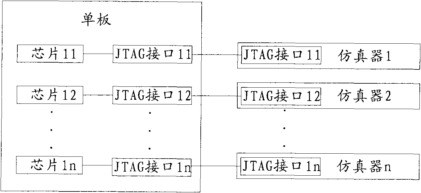
[0042] The JTAG switching interface in the embodiment of the present invention has all the signal functions of two or more different types of JTAG interfaces.

[0043] The JTAG transfer interface in this embodiment has all the signal functions of two or more different types of JTAG interfaces. Therefore, the JTAG transfer interface can support two or more different types of chips. The two or more different types of chips do not need to replace the JTAG transfer interface when debugging, which facilitates the debugging of the chip to a certain extent.

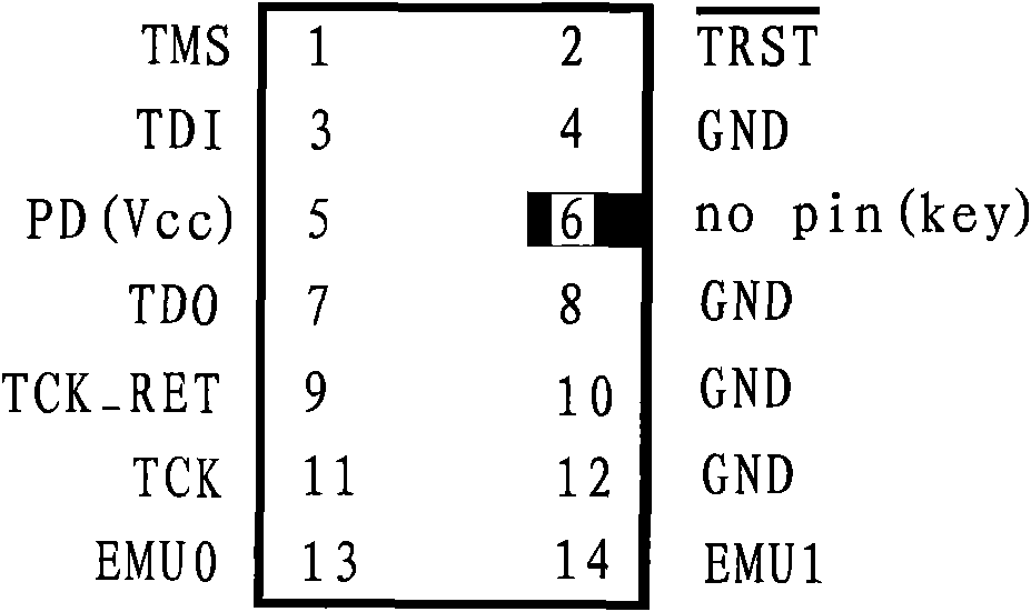
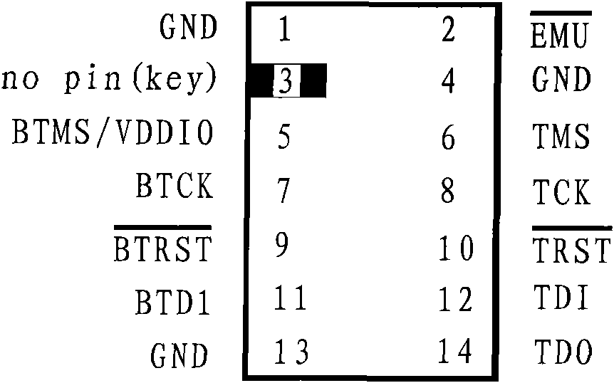
[0044] Such as Figure 4 As shown, how to integrate two different types of JTAG interfaces introduced by TI (Texas Instruments) and...


PUM


Abstract

The invention discloses a JTAG switching interface, a single board, a JTAG interface conversion board and a single board testing system, and relates to the communication technology field so as to bring convenience for adjusting a chip on the single board. The JTAG switching interface has all signal functions of two or more different JTAG interfaces. The single board comprises a printed circuit board which is provided with at least one chip connected with the JTAG switching interface. The JTAG switching interface has all signal functions of two or more different JTAG interfaces. The invention also discloses the JTAG interface conversion board and the single board testing system. The JTAG switching interface can be used for interface conversion.

Description

Technical field [0001] The invention relates to the field of communications, and in particular to a JTAG switching interface, a single board, a JTAG interface conversion board, and a single board testing system. Background technique [0002] At present, in order to understand and master the performance of a chip, it is generally necessary to use an emulator to perform hardware testing on it. The use of an emulator to test the chip requires connecting the two through an interface. Generally, the above interface uses the JTAG interface. JTAG (Joint Test Action Group, Joint Test Action Group) is a PCB (Printed Circuit Board, printed circuit board) and IC (Integrated Circuit, integrated chip) test standard initiated and formulated by several major international electronic manufacturers. It is mainly used in Boundary scan testing of circuits and internal testing of integrated chips. [0003] According to this standard, each company has launched its own JTAG interface and the e...

Claims


Application Information

Patent Timeline
IPC IPC(8): G01R31/28
Inventor 刘伟
Owner HUAWEI TECH CO LTD
Why Eureka
Try Eureka