Ohmic electrode structure and semiconductor element

An electrode structure, semiconductor technology, applied in the direction of semiconductor devices, electrical components, electrical solid devices, etc., can solve the problems of increased stress of the semiconductor layer 62, deterioration of device characteristics, etc., to reduce resistance, improve potential barrier performance, The effect of suppressing poor wire bonding

Inactive Publication Date: 2011-09-07
PANASONIC CORP
View PDF1 Cites 0 Cited by
  • Summary
  • Abstract
  • Description
  • Claims
  • Application Information

AI Technical Summary

Problems solved by technology

When the thickness of the barrier metal layer 66 is increased, the stress on the semiconductor layer 62 increases especially during high-output operation with a large amount of heat generation, and there is a risk of promoting the occurrence of defects and deteriorating device characteristics.

Method used


Image

  • Ohmic electrode structure and semiconductor element
  • Ohmic electrode structure and semiconductor element
  • Ohmic electrode structure and semiconductor element

Examples


Embodiment approach 1

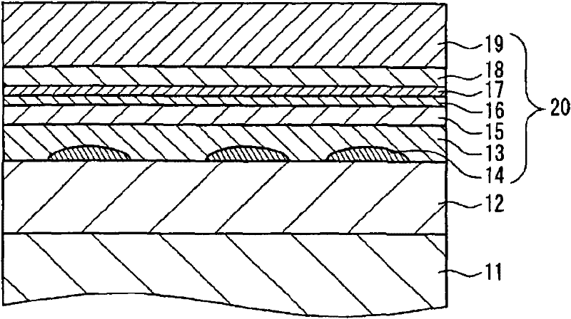
[0078] figure 1 It is a cross-sectional view schematically showing the electrode structure formed on the semiconductor layer in Embodiment 1 of the present invention. This electrode structure has an n-type GaAs contact layer (n-type semiconductor layer) 12 and an electrode metal layer (electrode) 20 formed on the n-type semiconductor layer. In this embodiment, an n-type electrode will be described as an example.

[0079] exist figure 1 In this example, on the n-type GaAs substrate 11, the n-type semiconductor layer 12 is formed as a contact layer with the electrode metal layer 20. An AuGeNi alloy layer 13 is formed on the n-type semiconductor layer 12 , and Ni14 is contained in the AuGeNi alloy layer 13 . On the AuGeNi alloy layer 13, the first Ti layer 15 is formed as the bonding metal layer of the first period. On the first Ti layer 15, the first Pt layer 16 is formed as a barrier metal layer of the first period. On the first Pt layer 16, a second Ti layer 17 is forme...

Embodiment approach 2

[0103] In the semiconductor element according to Embodiment 2 of the present invention, electrodes are formed on both the front surface and the back surface of the semiconductor element. As a semiconductor element having such a structure, there is, for example, a two-wavelength semiconductor laser device. Hereinafter, a dual-wavelength semiconductor laser device will be taken as an example for specific description.

[0104] Figure 5 It is a perspective view of the two-wavelength semiconductor laser device according to this embodiment seen from above. In the dual-wavelength semiconductor laser device according to this embodiment, a red semiconductor laser 1 having an oscillation wavelength in the 660 nm band and an infrared semiconductor laser 2 having an oscillation wavelength in the 780 nm band are formed on the same substrate.

[0105] Such as Figure 5 As shown, in the two-wavelength semiconductor laser device of this embodiment, a red semiconductor laser 1 and an infra...


PUM

PropertyMeasurementUnit
thicknessaaaaaaaaaa
thicknessaaaaaaaaaa
thicknessaaaaaaaaaa

Abstract

An ohmic electrode structure is provided with a AuGeNi alloy layer (13) arranged on an n-type GaAs layer; and a laminated body composed of bonded metal layers (15, 17) arranged on the AuGeNi alloy layer (13) and barrier metal layers (16, 18) arranged on the bonded metal layers (15, 17). The laminated body is arranged for two cycles or more. On a GaAs contact layer, especially on an n-type electrode, surface diffusion of Ga in the semiconductor and Ni in the AuGeNi alloy layer required for forming ohmic contact at the n-type electrode can be suppressed. Thus, the low resistance ohmic electrodestructure and a semiconductor element having such structure are provided.

Description

field of invention [0001] The present invention relates to an ohmic electrode structure of an n-type GaAs semiconductor layer and a semiconductor element using the electrode structure. Background technique [0002] In compound semiconductor devices such as semiconductor lasers and GaAs-based ICs, an ohmic electrode is often formed on an n-type GaAs layer. In an ohmic electrode, an alloy of AuGeNi is generally used as a metal capable of ohmic junction. For Ge, Ge in the AuGe of the ohmic electrode should consider the eutectic composition between Au and add about 12%, enter the Ga lattice node in the GaAs layer through alloying (alloying treatment), and become n-type doped miscellaneous agent. Therefore, the energy barrier between the AuGeNi layer and the n-type GaAs layer becomes low, enabling electron tunneling. [0003] On the other hand, Ni in the AuGeNi alloy is used to promote Ge diffusion whose diffusion rate is slow. Although the chemical free energy of GaAs decrea...

Claims


Application Information

Patent Timeline
Patent Type & Authority Patents(China)
IPC IPC(8): H01L21/28H01L33/00H01S5/042
CPCH01S5/0425H01L29/452H01S5/0421H01L2924/0002H01S5/04252H01L2924/00
Inventor 岛本敏孝吉川兼司牧田幸治
Owner PANASONIC CORP
Why Eureka
Try Eureka