Wireless device and manufacturing method of antenna thereof

A wireless device and manufacturing method technology, applied in the direction of antennas, electrical short antennas, antenna components, etc., can solve the problems of not effectively reducing the area occupied by PCB boards, reducing antenna transceiver performance, and wasting materials, so as to save materials, Improved transmission and reception performance and space-saving effects

Inactive Publication Date: 2010-02-03
HUAWEI DEVICE (SHENZHEN) CO LTD
View PDF2 Cites 5 Cited by
  • Summary
  • Abstract
  • Description
  • Claims
  • Application Information

AI Technical Summary

Problems solved by technology

[0005] The use of built-in antennas cannot effectively reduce the area occupied by the PCB board and waste materials, and b

Method used


Image

  • Wireless device and manufacturing method of antenna thereof
  • Wireless device and manufacturing method of antenna thereof
  • Wireless device and manufacturing method of antenna thereof

Examples


Embodiment Construction

[0021] The following will clearly and completely describe the technical solutions in the embodiments of the present invention with reference to the accompanying drawings in the embodiments of the present invention. Obviously, the described embodiments are only some, not all, embodiments of the present invention. Based on the embodiments of the present invention, all other embodiments obtained by persons of ordinary skill in the art without creative efforts fall within the protection scope of the present invention.

[0022] The technical solutions of the embodiments of the present invention will be further described below in conjunction with the accompanying drawings and specific embodiments.

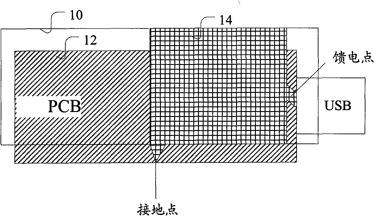
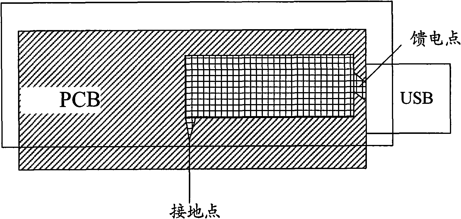
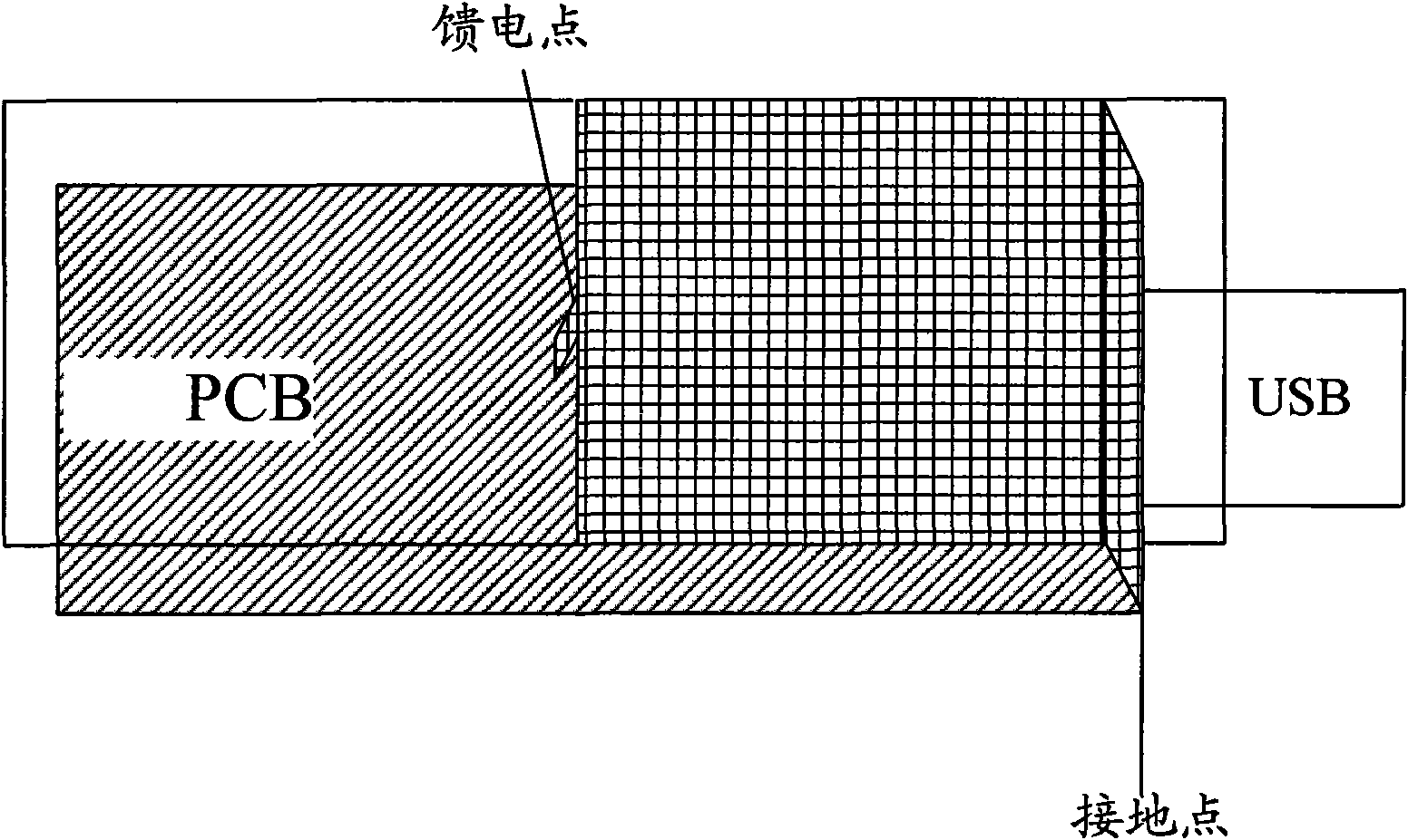
[0023] According to an embodiment of the present invention, a wireless device is provided. In the wireless device, the space between its casing and the PCB board is used as an antenna. In the following description, the above-mentioned antenna is called a loop antenna, figure 1 is a schem...


PUM


Abstract

The invention provides a wireless device and a manufacturing method of antenna thereof. The wireless device comprises a shell and a printed circuit board (PCB), wherein, a conducting material is applied to the inner side of the shell; one end of the conducting material is connected with a grounding point of the PCB, the other end of the conducting material is connected with a feed point of the printed circuit board; and the printed circuit board between the ground point and the feed point and the conducting material form the antenna of the wireless device. By the processing, the method saves materials and space of the built-in antenna on the PCB and improves the transceiving performance of the antenna.

Description

technical field [0001] Embodiments of the present invention relate to wireless communication technologies, and in particular, to a wireless device and a method for manufacturing an antenna of the wireless device. Background technique [0002] At present, the use of wireless data cards is becoming more and more popular. With the growth of people's needs, various functions need to be implemented in the limited space of wireless data cards, for example: on a printed circuit board (Printed Circuit Board; hereinafter referred to as: PCB) Realize multi-band and multi-system, realize Global Positioning System (Global Positioning System; hereinafter referred to as: GPS), realize storage function, realize digital video broadcasting (Digital Video Broadcasting; hereinafter referred to as: DVB) function, etc. Therefore, it is more and more difficult to layout various devices on a PCB with a limited area, which leads to an increasingly smaller environment for the built-in antenna of the...

Claims


Application Information

Patent Timeline
IPC IPC(8): H01Q1/24
CPCH01Q1/2275H01Q9/0421
Inventor 谢艳萍帅培华雷平班永灵杨兆良
Owner HUAWEI DEVICE (SHENZHEN) CO LTD
Why Eureka
Try Eureka