Bonding welding disk lowering parasitic capacitance and preparing method thereof

A technology for bonding pads and pads, applied in circuits, electrical components, electrical solid devices, etc., can solve problems such as pad metal layer peeling

Active Publication Date: 2011-06-15
SHANGHAI HUAHONG GRACE SEMICON MFG CORP
View PDF0 Cites 2 Cited by
  • Summary
  • Abstract
  • Description
  • Claims
  • Application Information

AI Technical Summary

Problems solved by technology

If the pad metal layer is only attached to the dielectric and is subjected to external pressure and tension from the bonding wire, the pad metal layer may peel off (peeling-off)

Method used


Image

  • Bonding welding disk lowering parasitic capacitance and preparing method thereof
  • Bonding welding disk lowering parasitic capacitance and preparing method thereof
  • Bonding welding disk lowering parasitic capacitance and preparing method thereof

Examples


Embodiment Construction

[0043] In order to make the object, technical solution and advantages of the present invention clearer, the present invention will be further described in detail below in conjunction with the accompanying drawings.

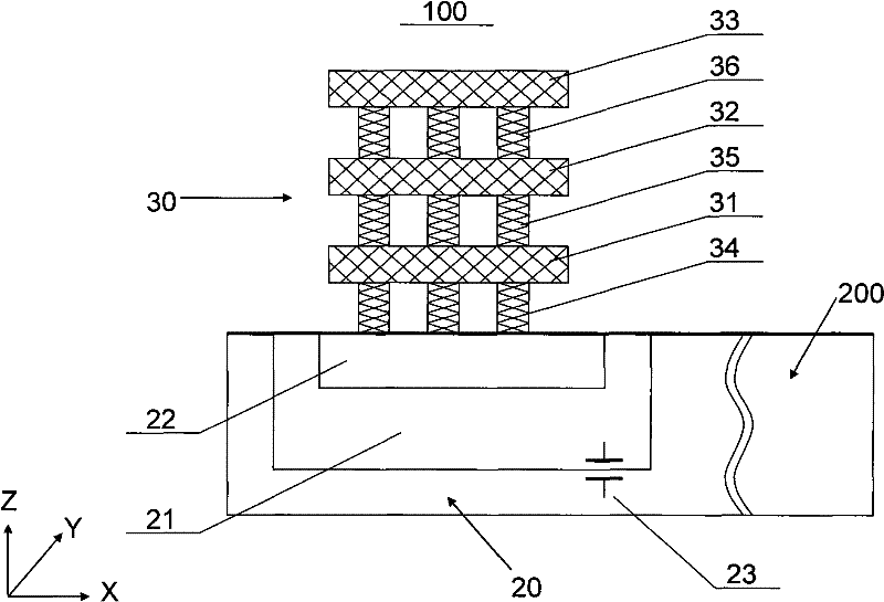
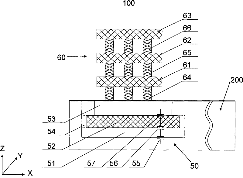
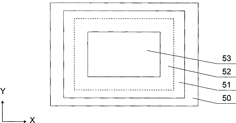
[0044] figure 2 Shown is a schematic structural diagram of the bonding pad provided by the present invention, defining the direction perpendicular to the upper surface of the semiconductor substrate as the Z direction, and the plane parallel to the upper surface of the semiconductor substrate as the XY plane. The bonding pad is included in the semiconductor substrate 50 and the pad metal layer 60 . The semiconductor substrate includes a semiconductor substrate (not shown) in the active device region and a semiconductor substrate 50 in the bonding pad region. On the region of the upper surface layer of the semiconductor substrate 50, a first semiconductor substrate is formed by semiconductor doping. The doped well region 51, the second semiconductor doped region ...


PUM

PropertyMeasurementUnit
thicknessaaaaaaaaaa
thicknessaaaaaaaaaa
thicknessaaaaaaaaaa

Abstract

The invention discloses a bonding welding disk lowering parasitic capacitance and a preparing method thereof, belonging to the technical field of manufacturing semiconductors. The bonding welding disk provided by the invention comprises a welding disk metal layer, a fist semiconductor doping well region, a second semiconductor doping zone and a first semiconductor high-doping zone, wherein, the fist semiconductor doping well region is formed by doping the semiconductor, the second semiconductor doping zone is formed in the fist semiconductor doping well region, and the first semiconductor high-doping zone is formed on the upper surface layer of the second semiconductor doping zone; junction capacitance formed between the first semiconductor doping well region and the second semiconductor doping zone, the junction capacitance formed between the second semiconductor doping zone and the first semiconductor high-doping zone and the junction capacitance formed between the first semiconductor doping well region and the semiconductor substrate are connected in series to lower the equivalent parasitic capacitance value of the bonding welding disk; meanwhile, the second semiconductor doping zone has simple preparing method and increases little cost of the preparing technology of the bonding welding disk.

Description

technical field [0001] The invention relates to the technical field of semiconductor manufacturing, in particular to a bonding pad for reducing parasitic capacitance and a preparation method thereof. Background technique [0002] In the technical field of semiconductor manufacturing, the electrical connection between the internal circuit and the external signal is completed through a bonding pad (Bond-Pad). If the pad metal layer is only attached to the dielectric and is subjected to external pressure and tension from the bonding wire, the pad metal layer may peel off (peeling-off). In order to avoid the occurrence of this peeling phenomenon, the pad metal layer must be tethered with the contact between the pad metal layer and the substrate, so that the substrate and the pad metal layer are electrically connected. [0003] There is a junction capacitance between the semiconductor substrate of the bonding pad and the semiconductor doped well region. Since the area of ​​the b...

Claims


Application Information

Patent Timeline
Patent Type & Authority Patents(China)
IPC IPC(8): H01L23/482H01L29/06H01L21/60
CPCH01L2224/16145
Inventor 黎坡张拥华周建华彭树根
Owner SHANGHAI HUAHONG GRACE SEMICON MFG CORP
Why Eureka
Try Eureka