Semiconductor structure and manufacturing method for same

a semiconductor and semiconductor technology, applied in the field of semiconductors, can solve the problems of increasing processing speed and power consumption, increasing the difficulty of semiconductor device manufacturing, and advancing toward the physical possible limit, so as to reduce parasitic capacitance, reduce parasitic capacitance, and improve electrical properties of semiconductor devices

Inactive Publication Date: 2019-12-12
SHANGHAI HUALI INTEGRATED CIRCUTE MFG CO LTD
View PDF8 Cites 2 Cited by
  • Summary
  • Abstract
  • Description
  • Claims
  • Application Information

AI Technical Summary

Benefits of technology

[0034]In a 28 nanometres and below node manufacturing process, the process for a gate side wall is particularly important, because it defines the position of a gate source / drain region relative to a gate, and decides the magnitude of the parasitic capacitance between a contact hole (CT) and the gate with regard to the following process for the contact hole. The semiconductor structure and the manufacturing method for same provided in the present disclosure reduce, by means of forming an air gap between two layers of side walls on the basis of this processing platform of fully depleted silicon-on-insulator, the dielectric value (K) of the material of the side wall, so that when a low K-value material (K<3) is used as a barrier substance between circuits, the parasitic capacitance value can be effectively reduced, which is, corresponding to the present disclosure, effectively reducing the parasitic capacitance between a contact hole and a gate. Therefore, the electrical properties of the semiconductor device are improved.

Problems solved by technology

Over 50 years, the dimension of semiconductors have been significantly reduced, which translates into an increasing processing speed and decreasing power consumption.
Semiconductor device manufacturing has therefore become increasingly challenging and advancing toward the physically possible limit.
With the continuous reduction in the size of super-large-scale integrated circuits, the limitations on processes and materials properties are increasingly significant, such that it is increasingly difficult to reduce the size of planar transistors.
In terms of reducing the parasitic capacitance, because of process limitations, it is difficult to reduce the parasitic capacitance value by means of geometry changes at present.

Method used


Image

  • Semiconductor structure and manufacturing method for same
  • Semiconductor structure and manufacturing method for same
  • Semiconductor structure and manufacturing method for same

Examples


Embodiment Construction

[0055]The present disclosure is described below in detail in conjunction with the accompanying drawings and particular embodiments. It is noted that the embodiments described in conjunction with the accompanying drawings and particular embodiments are merely exemplary, and should not be construed as any limitation on the scope of protection of the present disclosure.

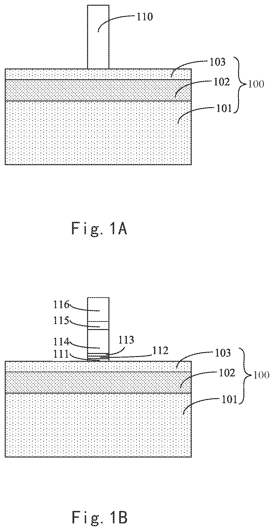
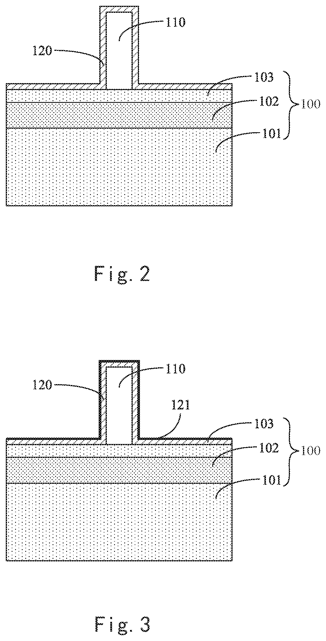
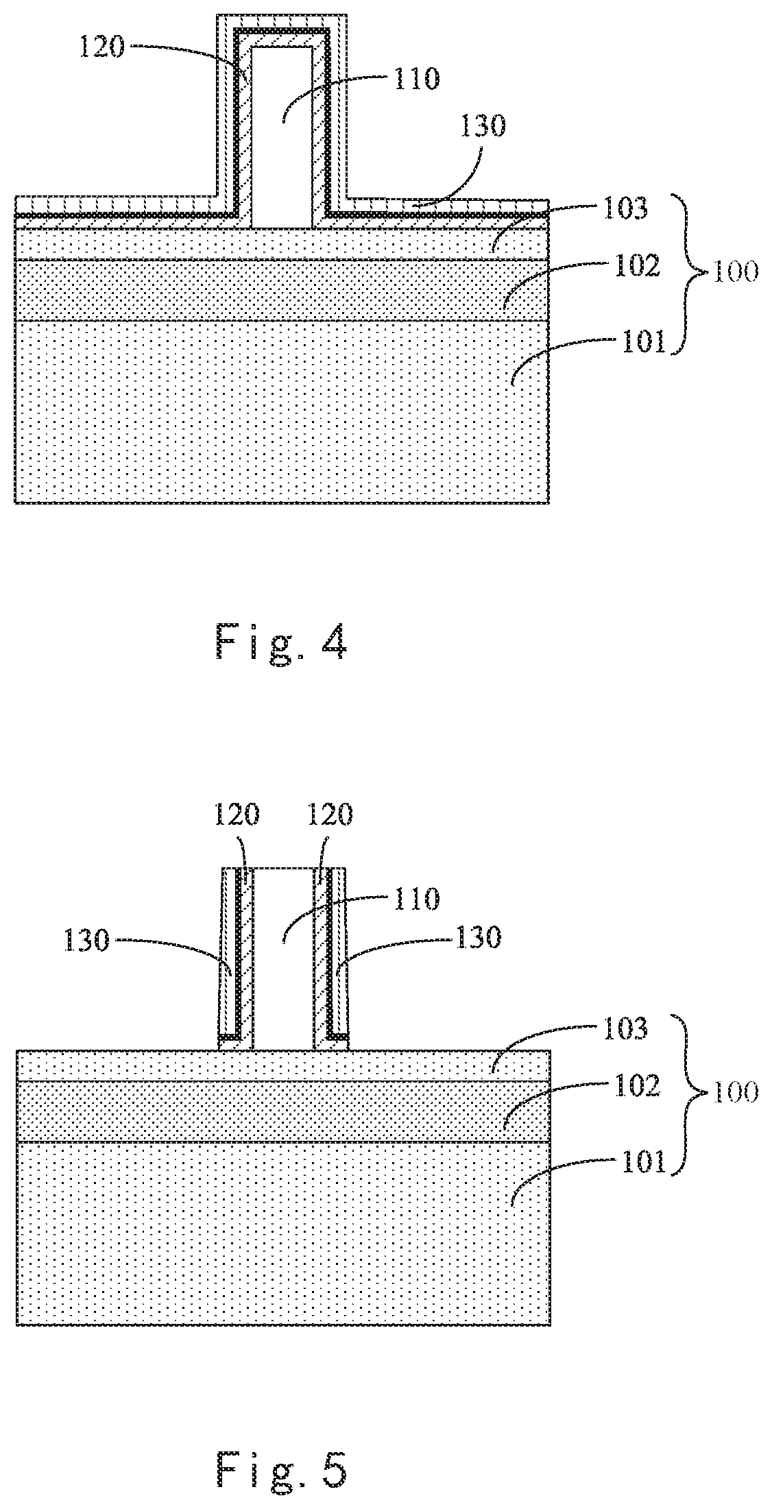
[0056]The present disclosure relates to a semiconductor process and device. More specifically, the embodiments of the present disclosure provide a semiconductor device. The semiconductor device comprises a substrate and a gate on the substrate, and silicon epitaxial layers are formed at two sides of the gate, a side surface of the gate is provided with a first side wall, with a gap being provided between the first side wall and the silicon epitaxial layer, and a surface of the first side wall is further provided with a second side wall for covering the gap, so that there is an air gap between the first side wall and the ...


PUM


Abstract

The present disclosure provides a semiconductor structure and a manufacturing method for the semiconductor structure. The semiconductor structure manufactured according to the manufacturing method provided in the present disclosure comprises a substrate and a gate formed on the substrate, and a silicon epitaxial layer is formed on the substrate at two sides of the gate; and a side surface of the gate is provided with a first side wall, with a gap being provided between the first side wall and the silicon epitaxial layer, and a surface of the first side wall further comprises a second side wall, with the second side wall covering the gap, so that there is an air gap between the first side wall and the silicon epitaxial layer.

Description

CROSS-REFERENCES TO RELATED APPLICATIONS[0001]The present application claims priority to Chinese Patent Application No. 201810581546.9, filed on Jun. 7, 2018, entitled “SEMICONDUCTOR STRUCTURE AND MANUFACTURING METHOD FOR SAME”, which is incorporated by reference herein for all purposes.TECHNICAL FIELD[0002]The present disclosure relates to the field of semiconductors, and in particular to the field of semiconductors of silicon-on-insulator.BACKGROUND OF THE DISCLOSURE[0003]Since the disclosure of integrated circuits by Dr. Jack Kilby of Texas Instruments in early years, scientists and engineers have made numerous disclosures and improvements in semiconductor devices and processes. Over 50 years, the dimension of semiconductors have been significantly reduced, which translates into an increasing processing speed and decreasing power consumption. To date, the development of semiconductors has largely followed Moore's Law, which roughly states that the number of transistors in dense i...

Claims


Application Information

Patent Timeline
Patent Type & Authority Applications(United States)
IPC IPC(8): H01L29/49H01L29/78H01L29/06H01L29/16H01L29/161H01L21/762H01L21/764H01L21/02H01L21/311
CPCH01L21/02274H01L21/31116H01L29/16H01L21/02164H01L29/7838H01L21/76289H01L21/02532H01L29/4991H01L21/02236H01L29/161H01L29/0649H01L21/0217H01L21/764H01L21/0228H01L21/823431H01L29/66795H01L29/785H01L29/6653H01L29/66545H01L29/6656H01L29/66628H01L29/66772H01L29/78618
Inventor SONG, YANGWANG, CHANGFENGLIAO, DUANQUAN
Owner SHANGHAI HUALI INTEGRATED CIRCUTE MFG CO LTD
Why Eureka
Try Eureka