

Liquid crystal display panel
A liquid crystal display panel and component technology, applied in the direction of static indicators, instruments, etc., can solve the problems of image quality deterioration, increase the number of driver integrated circuits, increase costs, etc., to improve display quality, solve flicker and uneven brightness The effect of the phenomenon
- Summary
- Abstract
- Description
- Claims
- Application Information
AI Technical Summary
Problems solved by technology
Method used
Image

Examples
no. 1 example
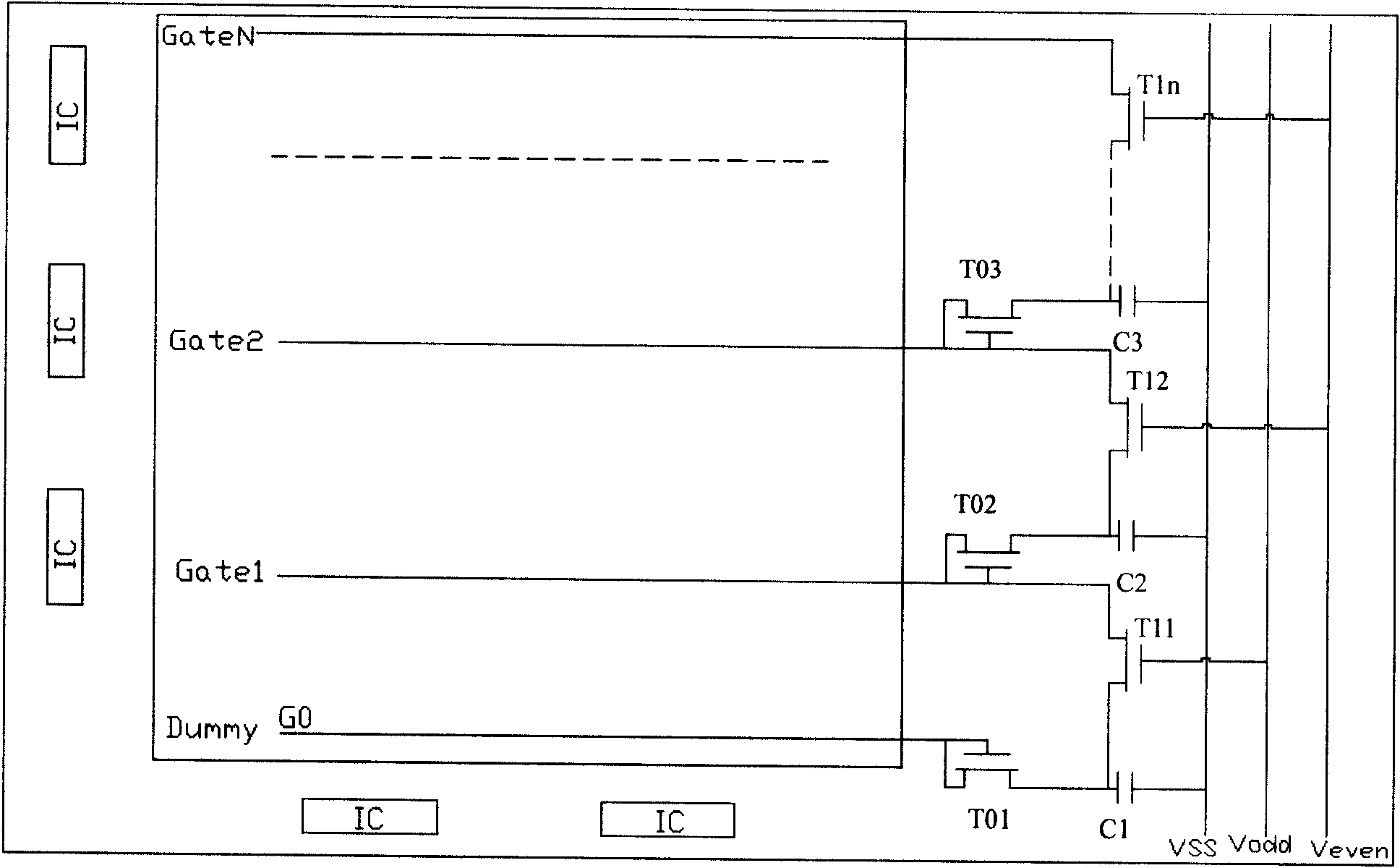
[0022] figure 2 It is a schematic structural diagram of a gate signal delay compensation device in a liquid crystal display panel according to the first embodiment of the present invention.
[0023] Such as figure 2 As shown, the liquid crystal display panel 1 includes a dummy gate line Dummy (G0) and a plurality of gate lines Gate1-GateN for transmitting gate signals, and also includes an odd level voltage Vodd and an even level voltage Veven for respectively Output different level signals. Corresponding to the plurality of gate lines, the liquid crystal display panel 1 includes a multi-level gate signal delay compensation device, which is respectively connected to the ends of the gate lines Gate1-Gaten at each level, wherein each level of compensation device includes a diode, a capacitor and a thin film transistor . The structures of the first-stage compensation device and the second-stage compensation device are described as examples. The first-stage compensation device ...
no. 2 example
[0027] Refer below Figure 4 A second embodiment of the present invention will be described. Figure 4 It is a structural schematic diagram of a liquid crystal display panel and a gate signal delay compensation device in the liquid crystal display panel according to the second embodiment of the present invention. Such as Figure 4 As shown, the difference between the second embodiment and the first embodiment is that the gate signal delay compensation devices of each stage further include a diode T21~T2n, and other components are the same as those of the first embodiment, using the same reference numerals. This will not be repeated here.
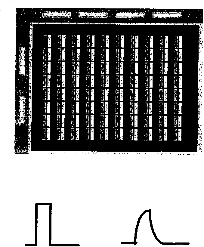
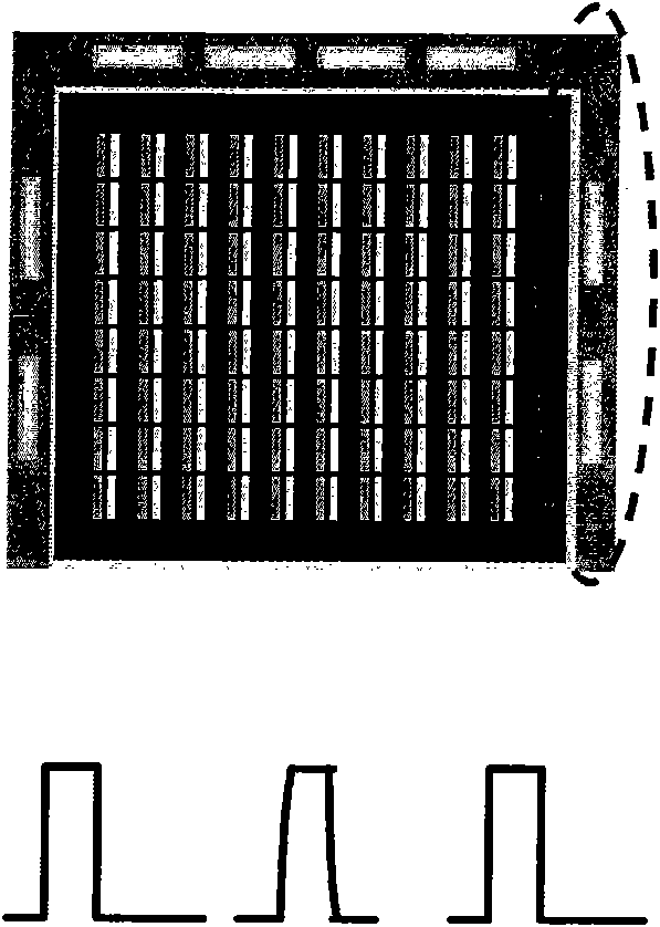
[0028] In the first embodiment, refer to figure 2 and image 3 As shown, when the odd-numbered row gate lines input high level, the odd-numbered level voltage Vodd is high-level, at this time, the thin-film transistors T11, T13, T15-T1n in the odd-numbered delay compensation device are turned on, and the input high level The other gate ...
no. 3 example
[0031] Refer below Figure 5 A third embodiment of the present invention will be described. Figure 5 It is a structural schematic diagram of a liquid crystal display panel and a gate signal delay compensation device in the liquid crystal display panel according to the third embodiment of the present invention. Such as Figure 5As shown, the difference between the third embodiment and the second embodiment is that the diodes T01~T0n in the delay compensation devices at all stages are replaced with thin film transistors TFT01~TFT0n, and the sources of the TFT01~TFT0n are connected to the high-level voltage VGH , components that are the same as those in the second embodiment use the same reference numerals, and will not be repeated here.
[0032] refer to Figure 5 This embodiment is described by taking the first-stage delay compensation device as an example. The first-stage delay compensation device includes a first thin film transistor TFT01, a capacitor C1, a second thin ...
PUM
 Abstract
Description
Claims
Application Information