

Alignment mark and defect detection method
A technology for alignment marks and defect detection, which is applied in the field of defect detection and can solve problems such as numerical offsets
- Summary
- Abstract
- Description
- Claims
- Application Information
AI Technical Summary
Problems solved by technology
Method used
Image

Examples
Embodiment Construction
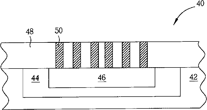
[0020] Please refer to figure 1 , figure 1 It is a schematic cross-sectional view of an alignment mark 40 in a preferred embodiment of the present invention. Such as figure 1 As shown, first a semiconductor substrate 42, such as a silicon wafer, is provided. An ion implantation process is then performed to implant N-type dopants into the semiconductor substrate 42 to form an N-type well (N-well) 44 . Then another ion implantation process is performed to implant P-type dopants into the formed N-type well 44 to form a shallower P+ doped region 46 in the N-type well 44 .
[0021] Then a dielectric layer 48 is formed on the semiconductor substrate 42 and covers the N − -type well 44 and the P+ doped region 46 . In this embodiment, the dielectric layer 48 may be made of dielectric materials such as oxides, carbides or nitrides, or low dielectric constant materials, or any combination thereof. Then form a patterned photoresist layer (not shown) on the dielectric layer 48, and u...
PUM
 Abstract
Description
Claims
Application Information