Novel non-vacuum adsorption wafer clamping mechanism

A clamping mechanism, non-vacuum technology, used in electrical components, semiconductor/solid-state device manufacturing, circuits, etc., and can solve problems such as small contact area

Inactive Publication Date: 2010-06-09
SHENYANG KINGSEMI CO LTD
View PDF0 Cites 20 Cited by
  • Summary
  • Abstract
  • Description
  • Claims
  • Application Information

AI Technical Summary

Problems solved by technology

The traditional vacuum adsorption method will directly contact the central area of ​​the wafer, so it becomes inapplicable in the double-sided coating development process, which requires the design of a method that does not require vacuum adsorption, and has a small contact area and avoids contact points. Open the clamping mechanism in the central process area

Method used


Image

  • Novel non-vacuum adsorption wafer clamping mechanism
  • Novel non-vacuum adsorption wafer clamping mechanism

Examples


Embodiment Construction

[0019] The present invention will be further described below in conjunction with the accompanying drawings and embodiments.

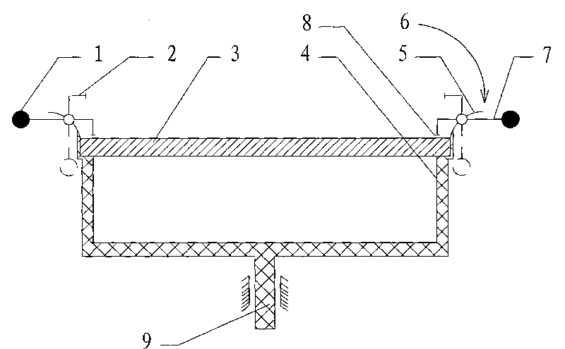
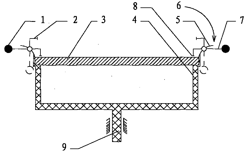
[0020] Such as figure 1 As shown, the non-vacuum suction wafer clamping mechanism of the present invention mainly includes a mechanism body 4 and a miniature lever mechanism 6, and a micro lever mechanism 6 for clamping the wafer 3 to be processed is provided around the mechanism body 4 of the wafer clamping mechanism. The micro-lever mechanism 6 is evenly distributed on the mechanism body 4 .

[0021] The wafer 3 to be processed is installed on the mechanism body 4, the edge of the wafer 3 to be processed is in contact with the mechanism body 4, the micro lever mechanism 6 is connected to the mechanism body 4 by the micro lever support 5, and the micro lever mechanism 6 is connected to the micro lever support 5 hinged.

[0022] The mechanism body 4 is an annular structure with a bottom surface. The bottom of the mechanism body 4 is provided with a ro...


PUM


Abstract

The invention relates to a novel non-vacuum adsorption wafer clamping mechanism belonging to the field of semiconductors. The novel non-vacuum adsorption wafer clamping mechanism is a wafer clamping mechanism arranged on semiconductor equipment and used during the rotating and processing of a wafer and especially used in an occasion which needs to protect the central figure area of the wafer and an occasion which can not supply vacuum or is inconvenient to use vacuum adsorption. The wafer clamping mechanism is provided with a mechanism body and a minitype lever mechanism, wherein the periphery of the mechanism body of the wafer clamping mechanism is provided with the minitype lever mechanism used for clamping the wafer to be processed. When a centrifuge rotates at a high speed, the clamping mechanism tightly clamps the wafer without generating the problems of wafter offset and desquamation during high-speed rotation. The wafer clamping mechanism has wide application range, is almost suitable for wafers in all shapes and sizes and only needs to change the position of the minitype lever mechanism and the size and the shape of a base with an annular bottom surface when the size and the shape of the processed wafer are changed.

Description

Technical field [0001] The invention relates to the field of semiconductors, specifically a new type of non-vacuum adsorption wafer clamping mechanism. In the semiconductor industry, the wafer holder used when rotary processing is required. When the process requires that the surface of the wafer cannot be directly in contact with the wafer holder, Or when it is inconvenient to provide vacuum adsorption, the structure of the present invention can be used to clamp the wafer to ensure that the rotating process can be performed normally. Background technique [0002] With the development of semiconductor technology and the needs of design, many processes now require double-sided film development, which requires that the process area of ​​the wafer cannot be contacted during processing. The traditional vacuum adsorption method will directly contact the central area of ​​the wafer, so it becomes inapplicable in the double-sided coating development process, which requires the desig...

Claims


Application Information

Patent Timeline
IPC IPC(8): H01L21/687
Inventor 王冲
Owner SHENYANG KINGSEMI CO LTD
Why Eureka
Try Eureka