LED display device
A technology for display devices and selection devices, applied to static indicators, instruments, etc., which can solve problems such as complex circuits, bright lights, and high cost
- Summary
- Abstract
- Description
- Claims
- Application Information
AI Technical Summary
Problems solved by technology
Method used
Image

Examples
Embodiment 1
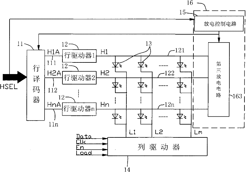
[0038] Such as figure 2 As shown, the scanning LED display device in the first embodiment of the present invention mainly includes a row decoder 11, a row driver 12, several rows of LEDs ( figure 2 Reference numeral 13), column driver 14, cascade circuit (not shown), discharge device 16, etc., will be described in detail below.
[0039] The several rows of LEDs can be arranged in a matrix. In the case of a relatively large display area, the LEDs can be arranged on several unit boards, such as on several circuit boards, and then assembled into a large display screen; In the case of a small screen, it can also be directly arranged on a substrate, such as a circuit board, and can also be arranged into display screens of various sizes according to needs. For illustrative purposes, figure 2 What is shown is the arrangement of some LEDs, and the actual situation is not limited thereto.
[0040] In this embodiment, eight rows of LEDs are used for ease of description; the decode...
Embodiment 2
[0060] On the basis of Example 1, 74LS139 can also be used as the discharge selection device, such as Figure 5 As shown, this embodiment takes the four-sweep unit board as an example for illustration. Pins 2 and 3 of the discharge selection device 74LS139 chip receive row selection signals HA, HB, and pins 14 and 13 also receive the above-mentioned row selection signals HA, HB, 1 Pin and pin 15 simultaneously receive the discharge selection signal CLOUTX as enable, pin 16 is connected to the working voltage VCC, pin 8 is grounded, and pins 1Y0, 1Y1, 1Y2, and 1Y3 are connected to row 124 and row 121 through the discharge device LED (number 18 in the figure). , 122 lines, 123 lines, similarly, 2Y0, 2Y1, 2Y2, 2Y3 are also connected to 124 lines, 121 lines, 122 lines, 123 lines in another group of LEDs through their corresponding discharge device LEDs, the discharge blanking mechanism and implementation Example 1 is the same and will not be repeated here.
[0061] The above 74LS...
Embodiment 3
[0063] On the basis of Example 1, CD4051B can also be used as the discharge selection device, such as Image 6 As shown, this embodiment takes the eight-sweep unit board as an example for illustration. Pins 11, 10, and 9 of the discharge selection device CD4051B chip receive row selection signals HA, HB, and HC, and pin 6 receives the discharge selection signal CLOUTX as an enable , 16 pins are connected to the working voltage VCC, 7 pins and 8 pins are grounded, 3 pins are grounded through a current limiting resistor, 1 pin is directly connected to 124 lines, 2 pins are directly connected to 126 lines, 4 pins are directly connected to 127 lines, 5 pins are directly connected to 125 lines 15 pins are directly connected to 122 rows, 14 pins are directly connected to 121 rows, 13 pins are directly connected to 128 rows, and 12 pins are directly connected to 123 rows.
[0064] 上述CD4051B也可以替换为74HC4051、74LS4051、74HCT4051、74ACT4051、CD54 / 74HC4051、CD54 / 74HCT4051、CD54 / 74HC4052、CD54 / 74H...
PUM
 Abstract
Description
Claims
Application Information
 - R&D Engineer
- R&D Manager
- IP Professional
- Industry Leading Data Capabilities
- Powerful AI technology
- Patent DNA Extraction
Browse by: Latest US Patents, China's latest patents, Technical Efficacy Thesaurus, Application Domain, Technology Topic.
© 2024 PatSnap. All rights reserved.Legal|Privacy policy|Modern Slavery Act Transparency Statement|Sitemap