Liquid crystal display device

A liquid crystal display device and liquid crystal layer technology, applied in nonlinear optics, instruments, optics, etc., can solve the problems of liquid crystal molecular orientation disorder, reduced manufacturing efficiency, and reduced contrast, and achieve fast response speed, improved manufacturing efficiency, and high brightness Effect

Inactive Publication Date: 2011-08-24
SHARP KK
View PDF2 Cites 2 Cited by
  • Summary
  • Abstract
  • Description
  • Claims
  • Application Information

AI Technical Summary

Problems solved by technology

[0013] However, in the liquid crystal display device having such slits or protrusions, there is a problem that an additional process for providing the slits or protrusions on the common electrode is required, and the production efficiency is reduced.
In addition, when coating an alignment film such as polyimide on the common electrode, a cleaning process is performed before and after the coating. However, when there are slits or protrusions, the alignment film may adhere to the slits or protrusions during cleaning. Dirt such as materials, the problem of alignment disorder of liquid crystal molecules occurs due to the dirt
When alignment disorder occurs, light leakage occurs during black display, causing problems such as display unevenness and contrast reduction

Method used


Image

  • Liquid crystal display device
  • Liquid crystal display device
  • Liquid crystal display device

Examples


Embodiment Construction

[0079] Hereinafter, embodiments of the liquid crystal display device of the present invention will be described with reference to the drawings.

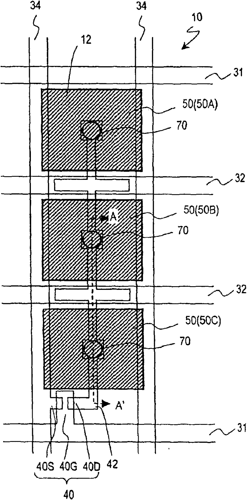
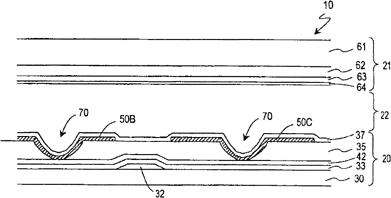
[0080] figure 1 is a plan view schematically showing the structure of one of the plurality of pixels 12 arranged in a matrix in the liquid crystal display device 10 of the present embodiment, figure 2 is a schematic representation of the liquid crystal display device 10 figure 1 A diagram of the shape of the A-A' cross-section.

[0081] In addition, in this specification, the minimum unit of display and the part corresponding to it are referred to as a pixel. For example, in a liquid crystal display device that performs color display using three colors R (red), G (green), and B (blue) , a pixel unit is composed of three pixels of R, G, and B. A pixel is defined as an area surrounded by two adjacent gate bus lines (scanning lines) and two adjacent source bus lines (signal lines) extending perpendicularly to the extending directi...


PUM

PropertyMeasurementUnit
diameteraaaaaaaaaa
depthaaaaaaaaaa
thicknessaaaaaaaaaa

Abstract

The invention discloses a liquid crystal display device, which performs high quality display with less display nonuniformity, excellent view angle characteristics and transmissivity, with high production efficiency. The liquid crystal display device is provided with a first substrate having a pixel electrode and an orientation film, a second substrate having a common electrode, and a liquid crystal layer arranged between the first substrate and the second substrate. The pixel electrode includes a plurality of subpixel electrodes which are electrically separated from each other on an insulating layer. The subpixel electrode has a recessed section which is recessed to the side of the insulating layer. The subpixel electrode and a drain line are connected at the recessed section, and the common electrode is formed substantially flat over the entire pixel electrode.

Description

technical field [0001] The present invention relates to a liquid crystal display device and a method for manufacturing the liquid crystal display device. Background technique [0002] Currently, liquid crystal display devices (LCDs) are widely used as display devices such as mobile phones, televisions, and computers. Among the currently popular horizontal alignment liquid crystal display devices, there are TN (Twisted Nematic: twisted nematic) mode liquid crystal display devices using nematic liquid crystal materials with positive dielectric constant anisotropy, STN (Super Twisted Nematic : Super twisted nematic) mode liquid crystal display device. [0003] In recent years, in order to improve viewing angle characteristics and display contrast, VAN (Vertical Aligned Nematic: Vertically Aligned Nematic) mode vertical alignment liquid crystal display devices have been developed and spread. [0004] Figure 5 It is a figure which shows the structure of the pixel part of the v...

Claims


Application Information

Patent Timeline
Patent Type & Authority Patents(China)
IPC IPC(8): G02F1/1343G02F1/1337
CPCG02F2001/133757G02F2001/134345G02F1/133753G02F1/1393G02F1/133757G02F1/134345
Inventor 望月雄贵秋友雅温千叶大
Owner SHARP KK
Why Eureka
Try Eureka