

Thin film transistor liquid crystal display (TFT-LCD) array substrate as well as manufacturing method and test method thereof
A technology of array substrate and manufacturing method, which is applied in the field of TFT-LCD array substrate and its manufacturing and testing, can solve problems such as inability to test signals in the liquid crystal panel, achieve the effect of enhancing the test analysis method and improving the comprehensive analysis ability
Active Publication Date: 2010-07-07
BOE TECH GRP CO LTD +1
View PDF0 Cites 45 Cited by
- Summary
- Abstract
- Description
- Claims
- Application Information
AI Technical Summary
Problems solved by technology
[0005] The purpose of the present invention is to provide a TFT-LCD array substrate and its manufacturing method and testing method. By addin
Method used
View moreImage
Smart ImageViewing Examples

Examples
 PUM
 Abstract
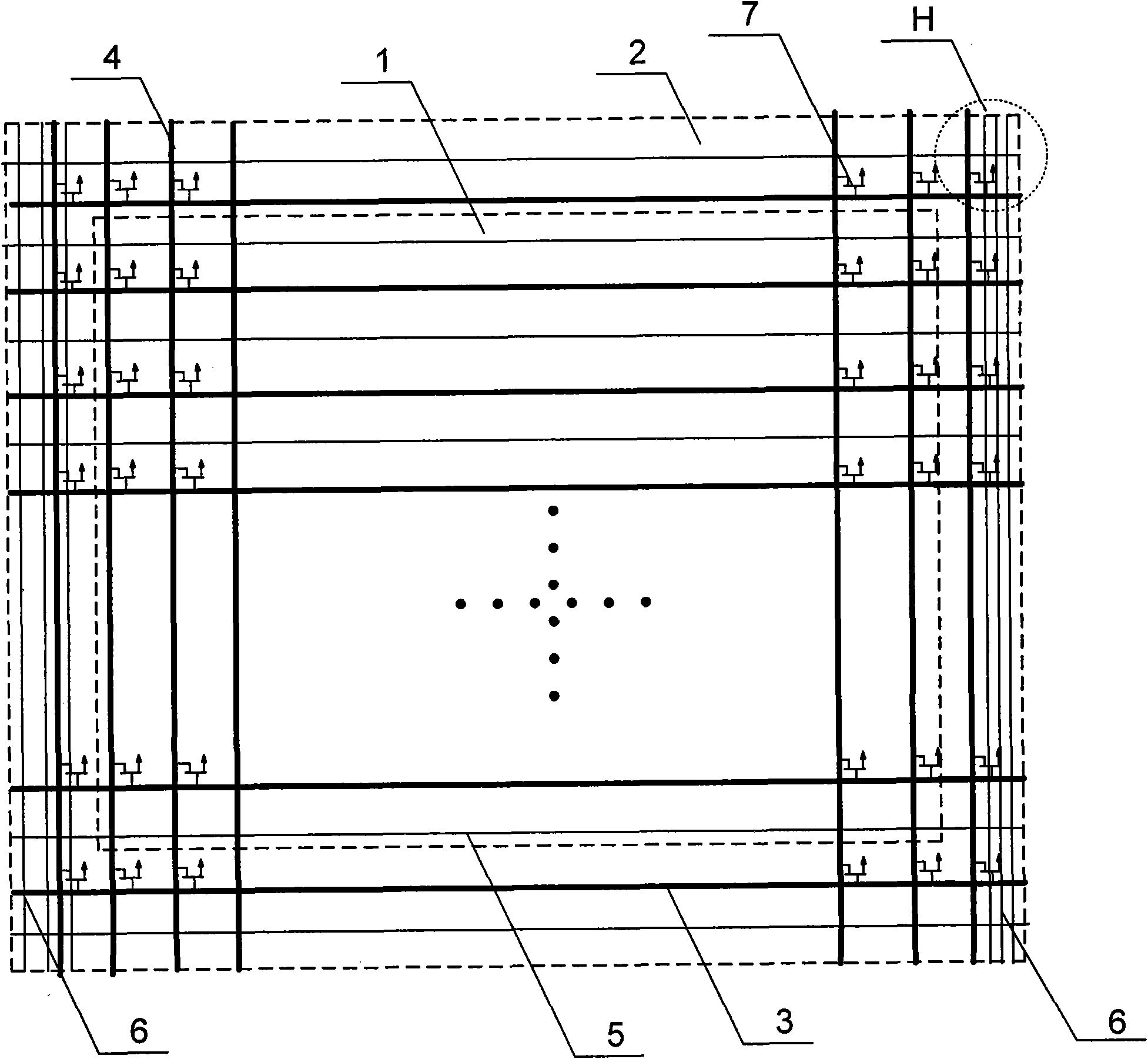
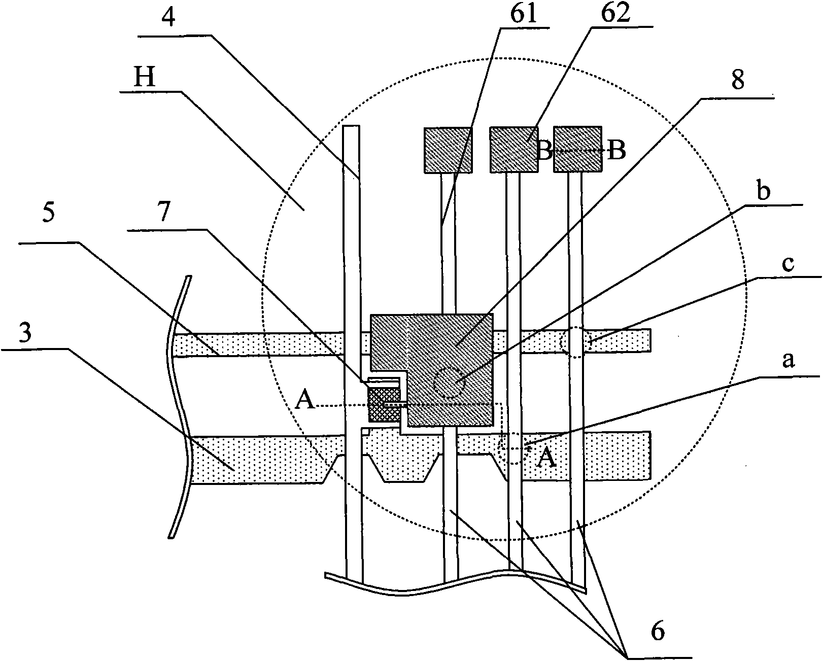
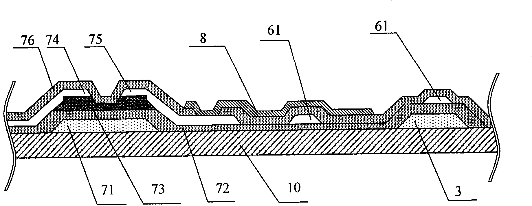
The invention relates to a thin film transistor liquid crystal display (TFT-LCD) array substrate as well as a manufacturing method and a test method thereof. TheTFT-LCD array substrate comprises a display area and a peripheral area, wherein the peripheral area is internally provided with at least one first testing line and/or at least one second testing line; the first testing lines are parallel to data lines; gate lines and/or pixel electrodes are overlapped with the at least one first testing line; the second testing lines are parallel to the gate lines; and the data lines are overlapped with the at least one second testing line. The invention effectively overcomes the technical defect that a signal inside a liquid crystal display panel can not be tested in the prior art by installing the test lines in the peripheral area.
Description
technical field [0001] The invention relates to a liquid crystal display device and its manufacturing method and testing method, in particular to a TFT-LCD array substrate and its manufacturing method and testing method. Background technique [0002] The main structure of Thin Film Transistor Liquid Crystal Display (hereinafter referred to as: TFT-LCD) includes a liquid crystal panel, a backlight and a driving circuit board. Finish. The liquid crystal panel is an opto-mechanical unity, and its basic principle is to use the electric field formed in the liquid crystal panel to control the deflection of the liquid crystal molecules, so that it produces different transmitted light under different electric fields. As a unified whole, it can be considered that the liquid crystal panel is the load of the driving circuit, and the liquid crystal molecules are the load of the electric field formed in the liquid crystal panel, and the three are a unified whole. [0003] The array sub...
Claims
Login to View More Application Information
Patent Timeline
 IPC IPC(8): G02F1/1362G02F1/13H01L21/84H01L27/12
Inventor赵继刚徐宇博
OwnerBOE TECH GRP CO LTD